Continue to Site

Welcome to EDAboard.com

Welcome to our site! EDAboard.com is an international Electronics Discussion Forum focused on EDA software, circuits, schematics, books, theory, papers, asic, pld, 8051, DSP, Network, RF, Analog Design, PCB, Service Manuals... and a whole lot more! To participate you need to register. Registration is free. Click here to register now.

Problem with LM35, ADC0804 and 89s52 interface (assembler code)

Status
Not open for further replies.

rvs

Junior Member level 1
Joined
May 10, 2012
Messages
17
Helped
0
Reputation
0
Reaction score
0
Trophy points
1,281
Activity points
1,440
I have a school project and I can't make it work correctly. I used diagram and code from this page http://www.eprlabs.com/2011/11/89s52-based-temperature-sensor-using-adc/. I added reset button, relay and ISP for programming. Now, the program shows values from 011 to 014 at room temperature (about 24 degrees in Celsius). Can anyone help me with writing the code, so it would work correctly? In the code I'm using right now, the relay isn't used at all.

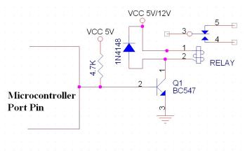
Picture of my diagram is here
**broken link removed**

Names of elements in diagram are not correct, because Eagle didn't have correct items and I used items, that had same size/number of legs/function for printig on board. I also added capacitor before and after 7805 voltage regulator.

I really need working code for this (code should activate realy at certain temperature).

Looking forward to solutions!

Raivo
 

I got it showing room temp with accuracy of +- 1 degree Celsius. I had left Vref unconnected.
Now I need a code, that would activate relay (for example) at 27 degrees Celsius. Can someone please write me a code that I could copy-paste to my original code?
 

Hello rvs,

Your LM35 can measure -55C to +150C with accuracy +1.5C and output scale 10mV/C. [for LM35 only. Different for LM35A/CA/C/D ]

Your ADC has 8-bit resolution with a maximum of 256 (28) steps. So, for Vref/2=1.28 Volt, you will get a full scale value for Vin=2.56Volt=2560mV. Remember that ADC has Vref/2 pin (pin 9). not Vref pin.
Now ADC will produce 0 for Vin=0 mV (0oC )
and will produce 256 for 2560 mV.

This has reference to ADC0804
 
Last edited:
  • Like
Reactions: rvs

    rvs

    Points: 2
    Helpful Answer Positive Rating
I put 1,28 V to pin 9 in ADC. I didn't realise that Vref/2 really means that Vref value has to be divided...I found correct value for Vref through testing and datasheets, where 2,56 and 1,28 V were mentioned as Vref (or Vref/2) values. But bigger problem is that I don't know assembler language and I can't write the pice of code for activating relay. Could someone please help me with that?
 

I put 1,28 V to pin 9 in ADC. I didn't realise that Vref/2 really means that Vref value has to be divided...I found correct value for Vref through testing and datasheets, where 2,56 and 1,28 V were mentioned as Vref (or Vref/2) values. But bigger problem is that I don't know assembler language and I can't write the pice of code for activating relay. Could someone please help me with that?

Suppose, LCD's E, R/W, RS connected to P2.2,P2.1 and P2.0. LCD's D0 to D7 connected to P1 port. And ADC output connected to P0.
Now the following code will display temperature.

[Output needs slight modification]


Code ASM - [expand]
1
2
3
4
5
6
7
8
9
10
11
12
13
14
15
16
17
18
19
20
21
22
23
24
25
26
27
28
29
30
31
32
33
34
35
36
37
38
39
40
41
42
43
44
45
46
47
48
49
50
51
52
53
54
55
56
57
58
59
60
61
62
63
64
65
66
67
68
69
70
71
72
73
74
75
76
77
78
79
80
81
82
83
84
85
86
87
88
89
90
91
92
93
94
95
96
97
98
99
100
101
102
103
104
105
106
107
108
109
110
org 0h
        RAM_ADDR EQU 30H
        COUNT EQU 3
 
        hundreds equ 30h
        tens equ 31h
        ones equ 32h
 
 
        ACALL DELAY_200M
        ACALL ONETIME_LCDINIT
 
STT: 
        ACALL ADC
        ACALL Bin2Dec
        ACALL DEC_ASCI_CONVRT
        ACALL DELAY_200M
        ACALL DELAY_200M
        ACALL DELAY_200M
        sjmp STT
 
;=================================================
;this subroutine is used to take data from ADC and
;keep to Accumulator
;=================================================
ADC: 
        mov A,P0
        nop
        nop
        ret
Bin2Dec:
        mov b,#100d
        div ab
        mov hundreds,a
        mov a,b
        mov b,#10d
        div ab
        mov tens,a
        mov ones,b
        ret 
 
DEC_ASCI_CONVRT: 
        MOV R0,#RAM_ADDR 
        MOV R2,#3 
BACKk:  MOV A,@R0 
        ORL A,#30H 
        ACALL DATA_DISPLAY
        INC R0 
        DJNZ R2,BACKk 
        RET
 
ONETIME_LCDINIT:
        MOV A,#38H 
        ACALL COMMAND 
        MOV A,#0EH 
        ACALL COMMAND 
        MOV A,#01H 
        ACALL COMMAND 
        MOV A,#06H 
        ACALL COMMAND 
        MOV A,#86H 
        ACALL COMMAND 
        RET
;;;;;;;;;;;;;;;;;;;;;;;;;;;;;;;;;;;;;;;;;
COMMAND:
        ACALL READY 
        MOV P1,A 
        CLR P2.0 
        CLR P2.1 
        SETB P2.2 
        CLR P2.2 
        RET
;;;;;;;;;;;;;;;;;;;;;;;;;;;;;;;;;;;;;;;;;
DATA_DISPLAY:
        ACALL READY 
        MOV P1,A 
        SETB P2.0 
        CLR P2.1 
        SETB P2.2 
        ACALL DELAY 
        CLR P2.2 
        RET
READY:  SETB P1.7 
        CLR P2.0 
        SETB P2.1 
BACK:   CLR P2.2 
        ACALL DELAY 
        SETB P2.2 
        JB P1.7,BACK 
        RET
;;;;;;;;;;;;;;;;;;;;;;;;;;;;;;;;;;;;;;;;;;;;;
DELAY_200M:
        MOV R7,#30H
        L1_DELAY: 
        MOV TMOD,#10
        MOV TH1,#3CH
        MOV TL1,#0B0H
        SETB TR1
        AGAIN: JNB TF1,AGAIN
        CLR TR1
        CLR TF1
        DJNZ R7,L1_DELAY
        RET
;;;;;;;;;;;;;;;;;;;;;;;;;;;;;;;;;;;;;;;;;;;;;
DELAY:  MOV R3,#50
HERE3:  MOV R4,#255 
HERE2:  DJNZ R4,HERE2
        DJNZ R3,HERE3
        RET
        END


Now To activate relay at 27C add the following code:

---------- Post added at 01:47 ---------- Previous post was at 00:52 ----------

----
-----
ACALL ADC
;Add the following two lines
CJNE A,#27, TRIPP
SETB P3.3 //or the pin connected to relay
TRIPP:
ACALL Bin2Dec
--------------
------------------
 
Last edited:
  • Like
Reactions: rvs

    rvs

    Points: 2
    Helpful Answer Positive Rating
LCD's RS (pin 4) goes to P3.4, R/W (pin 5) goes to GND and E (pin 6) goes to P3.5. LCD's D0 to D7 are connected to P2.0 to P2.7 in that order. ADC outputs are connected to P0.0 to P0.7.
If I want to use the code you have written here, I simply have to change port numbers t you have written to the ones that I really use? For example under command line you use P1,A; P2.0; P2.1; P2.2 and I should use P1,A (what is this?); P3.4; ??? (I put R/W to GND, but you assumed that I used P2.1 for R/W) ; P3.5?
 
Last edited:

If you want to use my code without any modification then connect:-

E -->P2.2
R/W -->P2.1 [explained below]
RS -->P2.0
ADC output -->P0 (port0)
LCD D0 to D7 -->port 1

There are 2 ways to send commands/data to LCD. --(1) Call a time delay before sending next data/command to an LCD (2) To monitor the busy flag before issuing a command / data to the LCD.

The READY subroutine follows the second method.
Note:- D7 bit of (command reg) LCD is busy flag which is connected to P1.7 of the microcontroller in my case(as D0 to D7 connected to port 1). To check that flag you need to make R/W=1 and RS=0 and a low to high pulse for the E pin. After that P1.7 reflects the state of busy flag.
When BF = 1 means LCD is busy and will not accept next command or data and BF = 0 means LCD is ready for the next command or data to process.


Code ASM - [expand]
1
2
3
4
5
6
7
8
9
10
11
12
READY: 
 
        SETB P1.7 ;To make P1.7 input port
        CLR P2.0 ;RS=0 to access command reg
        SETB P2.1 ;R/W = 1 to read command Reg
BACK: 
 
        CLR P2.2 ;E=0 to provide low to high pulse 
        ACALL DELAY ; give some time(pulse time)
        SETB P2.2 ; low to high pulse ends
        JB P1.7,BACK ; stay till busy flag=0
        RET


Hope this will throw some light.

58454d1310035107-vm.jpg

Picture of a working model
 
  • Like
Reactions: rvs

    rvs

    Points: 2
    Helpful Answer Positive Rating
I will try to change your code a bit, so it would match my connections. But I will do it tomorrow (it's about 3 am in my time and I'm too tired to change it right now). But if I do the small changes, could you please check my code and tell me, if it's correct for my program? I can't change where to connect LCD D0 to D7, so I have to change the code.
 

Ok no problem. I will be right here waiting for youuuuuuuuuuuuuuuuu.:-D
 

With my knowdledge I made this code

org 0h
RAM_ADDR EQU 30H
COUNT EQU 3

hundreds equ 30h
tens equ 31h
ones equ 32h


ACALL DELAY_200M
ACALL ONETIME_LCDINIT

STT:
ACALL ADC
ACALL Bin2Dec
ACALL DEC_ASCI_CONVRT
ACALL DELAY_200M
ACALL DELAY_200M
ACALL DELAY_200M
sjmp STT

;=================================================
;this subroutine is used to take data from ADC and
;keep to Accumulator
;=================================================
ADC:
mov A,P0 // ACD output to P.0
nop
nop
ret
Bin2Dec:
mov b,#100d
div ab
mov hundreds,a
mov a,b
mov b,#10d
div ab
mov tens,a
mov ones,b
ret

DEC_ASCI_CONVRT:
MOV R0,#RAM_ADDR
MOV R2,#3
BACKk: MOV A,@R0
ORL A,#30H
ACALL DATA_DISPLAY
INC R0
DJNZ R2,BACKk
RET

ONETIME_LCDINIT:
MOV A,#38H
ACALL COMMAND
MOV A,#0EH
ACALL COMMAND
MOV A,#01H
ACALL COMMAND
MOV A,#06H
ACALL COMMAND
MOV A,#86H
ACALL COMMAND
RET
;;;;;;;;;;;;;;;;;;;;;;;;;;;;;;;;;;;;;;;;;
COMMAND:
ACALL READY
MOV P2,A // LCD D0 to D7 connected to P2
CLR P3.4 // LCD RS (pin4) to P3.4
CLR P1.4 // LCD R/W (pin5) to P1.4 (I took unused port for this)
SETB P3.5 // LCD E (pin6) to P3.5
CLR P3.5
RET
;;;;;;;;;;;;;;;;;;;;;;;;;;;;;;;;;;;;;;;;;
DATA_DISPLAY: // I changed port numbres here
ACALL READY
MOV P2,A
SETB P3.4
CLR P1.4
SETB P3.5
ACALL DELAY
CLR P3.5
RET
READY: SETB P2.7
CLR P3.4
SETB P1.4
BACK: CLR P3.5
ACALL DELAY
SETB P3.5
JB P2.7,BACK
RET
;;;;;;;;;;;;;;;;;;;;;;;;;;;;;;;;;;;;;;;;;;;;;
ACALL ADC // added relay control correctly??
CJNE A,#27, TRIPP
SETB P1.3 // pin connected to relay
TRIPP:
ACALL Bin2Dec
RET // is this necessary??
;;;;;;;;;;;;;;;;;;;;;;;;;;;;;;;;;;;;;;;;;;;;;
DELAY_200M:
MOV R7,#30H
L1_DELAY:
MOV TMOD,#10
MOV TH1,#3CH
MOV TL1,#0B0H
SETB TR1
AGAIN: JNB TF1,AGAIN
CLR TR1
CLR TF1
DJNZ R7,L1_DELAY
RET
;;;;;;;;;;;;;;;;;;;;;;;;;;;;;;;;;;;;;;;;;;;;;
DELAY: MOV R3,#50
HERE3: MOV R4,#255
HERE2: DJNZ R4,HERE2
DJNZ R3,HERE3
RET
END


Sorry, I don't know how to insert the code like you did. I tried to attach .txt file but the attacher didn't upload my file.
 

Before going further, one comment about your relay connection.

Microcontrollers have internal pull up resistors hence when a port pin is HIGH the output current flows through this internal pull up resistor. 8051 microcontrollers have an internal pull up of 10KΩ. Now think that your base resistance R5 (in the given diagram **broken link removed** ) is not there. In that case the internal pull up of 10KΩ will act as a current limiter to base. Hence the maximum output current will be 5v/10k = 0.5ma. This current is not sufficient to drive the transistor into saturation and turn ON the relay.(we assume that R5 is not there. With it the current would be even lower) Hence an external pull up resistor is needed.
Let us now calculate the value of pull up resistance.
Normally a relay requires a pull in current of 70ma to be turned ON. So your BC547 transistor will require enough base current to make sure it remains saturated and provide the necessary collector current i.e. 70ma. The gain (hfe) of BC547 is 100 so you need to provide at least 70ma/100 = 0.7ma of base current. In practice you require roughly double the value of this current so we will calculate for 1.4ma of base current.

Base Current(1.4ma) =o/p current of controller (0.5ma) + 5v/R(value of pull up)
From the above equation the value of value of pull up comes out to be 5.55KΩ. Typically use 4.7KΩ resistor.

86_1245521291.jpg
 
  • Like
Reactions: rvs

    rvs

    Points: 2
    Helpful Answer Positive Rating
I can add that resistor easily, thank you for mentioning that!
But is the code I put here correct? I changed port/pin names to match my diagram, but I have no idea if should I change something else in that code?
 

Tried the code, but it shows 255->255255->255255255.... numbers don't start from left side, but from middle of the screen. What did I do wrong?

---------- Post added at 07:34 ---------- Previous post was at 07:33 ----------

I also tried

org 0h
RAM_ADDR EQU 30H
COUNT EQU 3

hundreds equ 30h
tens equ 31h
ones equ 32h


ACALL DELAY_200M
ACALL ONETIME_LCDINIT

STT:
ACALL Read_ADC
ACALL Bin2Dec
ACALL DEC_ASCI_CONVRT
ACALL DELAY_200M
ACALL DELAY_200M
ACALL DELAY_200M
ACALL TestTemperature
sjmp STT

;=================================================
;this subroutine is used to take data from ADC and
;keep to Accumulator
;=================================================
Read_ADC:
mov A,P0
nop
nop
ret
Bin2Dec:
mov b,#100d
div ab
mov hundreds,a
mov a,b
mov b,#10d
div ab
mov tens,a
mov ones,b
ret

DEC_ASCI_CONVRT:
MOV R0,#RAM_ADDR
MOV R2,#3
BACKk: MOV A,@R0
ORL A,#30H
ACALL DATA_DISPLAY
INC R0
DJNZ R2,BACKk
RET

ONETIME_LCDINIT:
MOV A,#38H
ACALL COMMAND
MOV A,#0EH
ACALL COMMAND
MOV A,#01H
ACALL COMMAND
MOV A,#06H
ACALL COMMAND
MOV A,#86H
ACALL COMMAND
RET
;;;;;;;;;;;;;;;;;;;;;;;;;;;;;;;;;;;;;;;;;
COMMAND:
ACALL READY
MOV P2,A
CLR P3.4
CLR P1.4
SETB P3.5
CLR P3.5
RET
;;;;;;;;;;;;;;;;;;;;;;;;;;;;;;;;;;;;;;;;;
DATA_DISPLAY:
ACALL READY
MOV P2,A
SETB P3.4
CLR P1.4
SETB P3.5
ACALL DELAY
CLR P3.5
RET
READY: SETB P2.7
CLR P3.4
SETB P1.4
BACK: CLR P3.5
ACALL DELAY
SETB P3.5
JB P2.7,BACK
RET
;;;;;;;;;;;;;;;;;;;;;;;;;;;;;;;;;;;;;;;;;;;;;
TestTemperature:
ACALL Read_ADC
CJNE A,#27,CheckFurther
RelayOn:
SETB P1.3
ret
CheckFurther:
jnc RelayOn
CLR P1.3
ret
;;;;;;;;;;;;;;;;;;;;;;;;;;;;;;;;;;;;;;;;;;;;;
DELAY_200M:
MOV R7,#30H
L1_DELAY:
MOV TMOD,#10
MOV TH1,#3CH
MOV TL1,#0B0H
SETB TR1
AGAIN: JNB TF1,AGAIN
CLR TR1
CLR TF1
DJNZ R7,L1_DELAY
RET
;;;;;;;;;;;;;;;;;;;;;;;;;;;;;;;;;;;;;;;;;;;;;
DELAY: MOV R3,#50
HERE3: MOV R4,#255
HERE2: DJNZ R4,HERE2
DJNZ R3,HERE3
RET
END

This code I got with help from another forum. Result was the same.
 

I can add that resistor easily, thank you for mentioning that!
But is the code I put here correct? I changed port/pin names to match my diagram, but I have no idea if should I change something else in that code?

The final code will be like the following:-


Code ASM - [expand]
1
2
3
4
5
6
7
8
9
10
11
12
13
14
15
16
17
18
19
20
21
22
23
24
25
26
27
28
29
30
31
32
33
34
35
36
37
38
39
40
41
42
43
44
45
46
47
48
49
50
51
52
53
54
55
56
57
58
59
60
61
62
63
64
65
66
67
68
69
70
71
72
73
74
75
76
77
78
79
80
81
82
83
84
85
86
87
88
89
90
91
92
93
94
95
96
97
98
99
100
101
102
103
104
105
106
107
108
109
110
111
112
113
114
115
org 0h
        RAM_ADDR EQU 30H
        COUNT EQU 3
 
        hundreds equ 30h
        tens equ 31h
        ones equ 32h
 
 
        ACALL DELAY_200M
        ACALL ONETIME_LCDINIT
 
STT: 
        ACALL ADC
        CJNE A,#27, TRIPP        ; If not equal to 27 go to TRIPP to show temperature
        SETB P1.3                        ; If equal to 27 activate relay and show temperature
TRIPP:
        ACALL Bin2Dec
        ACALL DEC_ASCI_CONVRT
        ACALL DELAY_200M
        ACALL DELAY_200M
        ACALL DELAY_200M
        SJMP STT
 
;=================================================
;this subroutine is used to take data from ADC and
;keep to Accumulator
;=================================================
ADC: 
        mov A,P0 // ACD output to P.0 
        nop
        nop
        ret
Bin2Dec:
        mov b,#100d
        div ab
        mov hundreds,a
        mov a,b
        mov b,#10d
        div ab
        mov tens,a
        mov ones,b
        ret 
 
DEC_ASCI_CONVRT: 
        MOV R0,#RAM_ADDR 
        MOV R2,#3 
        BACKk: MOV A,@R0 
        ORL A,#30H 
        ACALL DATA_DISPLAY
        INC R0 
        DJNZ R2,BACKk 
        RET
 
ONETIME_LCDINIT:
        MOV A,#38H 
        ACALL COMMAND 
        MOV A,#0EH 
        ACALL COMMAND 
        MOV A,#01H 
        ACALL COMMAND 
        MOV A,#06H 
        ACALL COMMAND 
        MOV A,#86H 
        ACALL COMMAND 
RET
;;;;;;;;;;;;;;;;;;;;;;;;;;;;;;;;;;;;;;;;;
COMMAND:
        ACALL READY 
        MOV P2,A // LCD D0 to D7 connected to P2 
        CLR P3.4 // LCD RS (pin4) to P3.4 
        CLR P1.4 // LCD R/W (pin5) to P1.4 (I took unused port for this) 
        SETB P3.5 // LCD E (pin6) to P3.5 
        CLR P3.5 
        RET
;;;;;;;;;;;;;;;;;;;;;;;;;;;;;;;;;;;;;;;;;
DATA_DISPLAY: // I changed port numbres here
        ACALL READY 
        MOV P2,A 
        SETB P3.4 
        CLR P1.4 
        SETB P3.5 
        ACALL DELAY 
        CLR P3.5 
        RET
READY: 
        SETB P2.7 
        CLR P3.4 
        SETB P1.4 
BACK: 
        CLR P3.5 
        ACALL DELAY 
        SETB P3.5 
        JB P2.7,BACK 
        RET
 
DELAY_200M:
        MOV R7,#30H
        L1_DELAY: 
        MOV TMOD,#10
        MOV TH1,#3CH
        MOV TL1,#0B0H
        SETB TR1
AGAIN:  JNB TF1,AGAIN
        CLR TR1
        CLR TF1
        DJNZ R7,L1_DELAY
        RET
;;;;;;;;;;;;;;;;;;;;;;;;;;;;;;;;;;;;;;;;;;;;;
DELAY:  MOV R3,#50
HERE3:   MOV R4,#255 
HERE2:   DJNZ R4,HERE2
        DJNZ R3,HERE3
        RET
        END


---------- Post added at 12:33 ---------- Previous post was at 12:29 ----------

Change the '//' to ';' to make comment
 

I will try it in 10-15 min!

---------- Post added at 08:09 ---------- Previous post was at 08:06 ----------

Still shows 255->255255->255255255...

---------- Post added at 08:11 ---------- Previous post was at 08:09 ----------

I changed '//' to ';' before i tried the code. That I figured out on my own :D
 

With a digital multimeter check the voltage of pin 6(Vin+) and pin 9(Vref/2) of the adc. Also let me know the current temperature at your place.
 

Room temp 24,9 degrees Celsius. pin 9 1,262 V and pin 6 was 0,262 V

---------- Post added at 09:52 ---------- Previous post was at 08:46 ----------

I changed pin 9 to 1,28 V. It doesn't have to be 100% accurate, but it has to work.
 

Make the following change:-


Code ASM - [expand]
1
2
3
4
RAM_ADDR EQU 30H
        COUNT EQU 2
        tens equ 30h
        ones equ 31h


Code ASM - [expand]
1
2
3
4
5
6
7
8
9
10
11
12
13
14
15
16
17
Bin2Dec:
            mov b,#10d
            div ab
            mov tens,a
            mov ones,b
            ret 
 
DEC_ASCI_CONVRT: 
                MOV R0,#RAM_ADDR 
                MOV R2,#2 
BACKk: 
        MOV A,@R0 
                ORL A,#30H 
                ACALL DATA_DISPLAY
                INC R0 
                DJNZ R2,BACKk 
         RET


It now shows 95->9595->959595->95959595....

And it's adding numbers to previous numbers. With the first code I used, it cleared display each time and showd only one number. Is it intentional that it does like that?

---------- Post added at 10:28 ---------- Previous post was at 10:17 ----------

And changing Vref value has no effect on result value (it's constant on 95)
 

If you can give me the C code of the above project then I can give you the completed project files. I will be using mikroC PRO for 8051 Compiler. Just give the C Source code and get the asm file from me.
 

Status
Not open for further replies.

Similar threads

Part and Inventory Search

Welcome to EDABoard.com

Sponsor

Back
Top