Continue to Site

Welcome to EDAboard.com

Welcome to our site! EDAboard.com is an international Electronics Discussion Forum focused on EDA software, circuits, schematics, books, theory, papers, asic, pld, 8051, DSP, Network, RF, Analog Design, PCB, Service Manuals... and a whole lot more! To participate you need to register. Registration is free. Click here to register now.

[SOLVED] Problem with Inverter

Status
Not open for further replies.

Mohammad Zubair

Junior Member level 3
Joined
Jan 13, 2015
Messages
25
Helped
0
Reputation
0
Reaction score
0
Trophy points
1
Activity points
214
67_1288131834.jpg

Hi
I am using the following circuit of inverter. I have some problems coming:

1) I get a 15V peak and 30V p-p sine wave (by further employing a RC filter) circuit when I apply a DC Bus Voltage of +30V. Shouldn't I be getting a peak voltage of +30V. Please Do guide me !!

2) My IGBTs get very hot even at a DC Bus Voltage of +30V. I am using a PWM frequency of 15khz. My IGBTs also draw very large current from the DC Bus. I put a load of 5k ohms but still current from the DC Bus is 0.7A.

I also included a Dead time of 10us to ease the heating problem but its still getting a lot of heat up and problem is there.

My IGBTs= IRG4BC20KD

Thanking in Advance!!!!
 

Hi,

try to connect schottky diodes in parallel to the gate drive resistors. both cathode in direction to driver.

Klaus
 

I did that that and also grounded the 11 pin of ir2112 ic
It smoothed my sine wave. However IGBTS still getting pretty HOT
 

Hi,

add a bulk capacitor at VCC. No standard electrolytic but a tantal one. Maybe 100uF. An additional 1uF ceramic may improve stability.
This ensures fast charge of bootstrap capacitor.

then try to short R10, R7, and R1.
Keep the wires/traces to the gate drive short and wide.


Klaus
 

I also have tried shorting these resistors in my real circuit, however still there is no effect of lessening of heating of IGBTs.

However, I have not used a Bulk Capacitor. I will try it and reply you with the result tomorrow. I hope it will decrease the heating of IGBTs
 

With 30VDC supply you can max 30V P-P output, so you are ok with this.
The reason for the IGBT getting hot is that the 2 gates are high together for part of the time. It could be the output of the microcontroller or delays in the gate drive. You can check that with an oscilloscope or with DMM measuring DC voltage between the 2 gates, it should be only few millivolts.
 

Thanks for the reply. But I didn't get the point " measuring DC voltage between the 2 gates".

should I be measuring voltage between the two gates?? (with one terminal of dmm on one gate and other terminal on the orther's gate)

What will it mean?? Can you clarify it a bit please??
 

You can also add a snubber circuit near to each switching device.
This will reduce the peak current flowing inside during opening period.

Another possibility, but it's kind of hard to evaluate without a notion either of the waveform or the board layout, is that the transistor base is receiving induced noise, which could cause undesired DC driving during the period that should be with zero logical level.
 

Because the gates have opposite phase the average voltage between them is 0V, if one drive is wrong then you get either positive or negative voltage. This method of checking the gates signal is very inaccurate.
If the microcontroller outputs are giving delays for on and no delay for off (most PWM do), these delays will cause overlapping by reversing the polarity of the signals by the optocouplers. Overlapping of the gates drives will cause the IGBTs to conduct together and overheat.
Try adding logic inverters or connecting the microcontroller outputs directly to the IR2112.
 

If that's the case then the output waveform should have some noise too
My output sinewave is very good without any noise or so
 

and regarding the 30V p-p, I have some confusions.

When my hi side IGBT is on and lo side is off, I should get my all 30 V on output in the first half cycle of sine wave.
an when switching starts to take place on the lo side IGBT, I should get all my 30 V as negative voltage....

Isn't it the case??????????
Please Clarify???
Thanking in advance :)
 

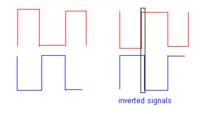
I've illustrated the drive signals to show what I mean. The left shows signals that are never high together to avoid IGBT conducting together. This is normal signals from M/C.
On the right the signals are inverted as your optocoupler does. I marked the area that the IGBTs will conduct together.
I think this could be your problem.
 

I have solved issues with my inverter. @Vbase, I implemented your advice and now it seems to be working fine.
 

Status
Not open for further replies.

Similar threads

Part and Inventory Search

Welcome to EDABoard.com

Sponsor

Back
Top