Continue to Site

Welcome to EDAboard.com

Welcome to our site! EDAboard.com is an international Electronics Discussion Forum focused on EDA software, circuits, schematics, books, theory, papers, asic, pld, 8051, DSP, Network, RF, Analog Design, PCB, Service Manuals... and a whole lot more! To participate you need to register. Registration is free. Click here to register now.

problem with differential pair

Status
Not open for further replies.

ahmad1954

Full Member level 4
Full Member level 4
Joined
Jun 30, 2012
Messages
192
Helped
26
Reputation
52
Reaction score
26
Trophy points
1,308
Visit site
Activity points
2,102
I want to calculate linear range of a simple mos differential pair with hspice. this is my netlist:

Vdc1 1 6 0
vcm 6 0 3
VCC 11 0 DC 5
VDD 12 0 DC -5
M1 3 1 5 5 NMOS1 w=10u l=.1u
M2 4 6 5 5 NMOS1 w=10u l=.1u
RC1 11 3 1k
RC2 11 4 1k
RE 5 12 7.2K
.MODEL NMOS1 Nmos level=2
.print dc id(m1) id(m2)
.dc vdc1 -3 3 1m

and this is output:
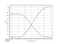

my question is why 2 graphs are not symmetric?
 

if you look at netlist you see that all values for resistors and transistors are same.
 

By process of elimination I would say issue is in gate connections. Does Vdc1 have a default source resistance?
 

so what should I do for symmetric output? should I apply another source to M2 gate? in this case which source should vary for calculating linearity range?
 

please tell me if I'm wrong. I should apply 2 sources to transistors gate and perform 2 dc sweep with conditions that you said. is this true?
 

I would probably use a voltage controlled voltage source to produce the other voltage - you want the results in a single sweep. See attached.

Keith
 

Attachments

  • Diff amp.pdf
    7 KB · Views: 73
What software did you use?
I tried your idea in hspice and I received this error: **error** inductor/voltage source loop found containing 0:vdc1 defined in subckt 0

this is new code:
Vdc1 1 6 0
vcm 6 0 3
VCC 11 0 DC 5
VDD 12 0 DC -5
M1 3 1 5 5 NMOS1 w=10u l=.1u
M2 4 7 5 5 NMOS1 w=10u l=.1u
RC1 11 3 1k
RC2 11 4 1k
RE 5 12 7.2K
E1 1 6 6 7 1
.MODEL NMOS1 Nmos level=2
.print dc id(m1) id(m2)
.dc vdc1 -3000m 3000m 1m
 

I think your E1 is incorrect. HSPICE has output nodes first then input nodes. Try E1 7 6 6 1 1

I use SIMetrix, but the simulator shouldn't matter - it should work any any SPICE simulator (with slight syntax differences).

Keith
 
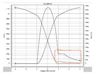
now I want to calculate GM. by definition I should calculate d(Iout). the output is shown below:


my question is why the red rectangle in the right of the figure is this form?
 

Hi ahmad1954,
just for a better understanding of the differential pair:

Your output characteristics would exhibit better symmetry - even if you apply one single input voltage only - if you reduce the common mode gain by increasing the common emitter resistance.
An ideal diff. pair has a current source in the emitter path (resistance approaching infinite) with a nearly ideal common mode rejection ratio and symmetrical output curves.
 

For a differential pair I would have thought you would want diff(Id1-Id2)/diff(Vg1-Vg2) but it depends on what your objective is. Your syntax might be slightly different to mine (DERIV for HSPICE I think). I don't see any strange discontinuities doing that and the gm tails off rather than making an abrupt drop to zero which is what yours seems to do.

Keith.
 

Attachments

  • Diffamp gm.pdf
    5.3 KB · Views: 86

Status
Not open for further replies.

Part and Inventory Search

Welcome to EDABoard.com

Sponsor

Back
Top