Continue to Site

Welcome to EDAboard.com

Welcome to our site! EDAboard.com is an international Electronics Discussion Forum focused on EDA software, circuits, schematics, books, theory, papers, asic, pld, 8051, DSP, Network, RF, Analog Design, PCB, Service Manuals... and a whole lot more! To participate you need to register. Registration is free. Click here to register now.

Problem with charactersics of Wilkinson Power Divider

Status
Not open for further replies.

mr_evo

Junior Member level 1
Joined
Nov 22, 2013
Messages
15
Helped
1
Reputation
2
Reaction score
1
Trophy points
3
Visit site
Activity points
96
Good afternoon!
Recently I've calculated WPD parameters. Then it was obtained simulation results of schematic circuit. Now I'm trying to create the structure in field representation, but simulation results are different. What can be the reason?
please have a look on attached pictures. s-parameters.JPG3d.JPG3dsparam.JPG
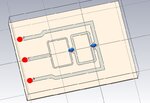
I think output lines make the influence. How to reduce it?
 
Last edited:

Try to place port 2 and port 3 on the PCB, opposite to port 1, and making their traces shorter.
 

I don't know the topology you used. Usually the input and the two outputs are on the opposite sides of the board, so the two rings are not internal to the structure.
How did you model in you circuit the coupling between loops and external traces ?
However I don't think the problem is due to the input/output lines; I presume their width is calculated to have 50 ohm impedance.
 

I need port 2 and 3 exactly in this positions.

How did you model in you circuit the coupling between loops and external traces ?
I didn't take it into account, that's why such unexpected characteristics were obtained.

However I don't think the problem is due to the input/output lines; I presume their width is calculated to have 50 ohm impedance.
You are right, width is calculated to 50ohm impedance.

I tried different length of the external traces and mentioned that s-parameters depend on it.
If I increase length in x-axis then it occures bigger attenuation of S22, S33 in lower frequency band. Increasing of the length in y axis leads to increasing attenuation of S11 in lower band, but S22, S33 in this case become equal in both bandwidth.
 

yes the lines for the two outputs, closest to the resistor, are very close to the lines of the splitter. There is probably some coupling. Also you did not chamfer those output line right angle bends. Spread things out!
 

yes the lines for the two outputs, closest to the resistor, are very close to the lines of the splitter. There is probably some coupling. Also you did not chamfer those output line right angle bends. Spread things out!
After some manipulations with this outputs, it was obtained better characteristics, but not ideal (which was in schematic simulation). How to calculate this angle bends in the right way? What I found in Pozar book is only that the length of chamfered bends (A) usually =1.8W.chamfer bends.JPG
 

Status
Not open for further replies.

Part and Inventory Search

Welcome to EDABoard.com

Sponsor

Back
Top