Continue to Site

Welcome to EDAboard.com

Welcome to our site! EDAboard.com is an international Electronics Discussion Forum focused on EDA software, circuits, schematics, books, theory, papers, asic, pld, 8051, DSP, Network, RF, Analog Design, PCB, Service Manuals... and a whole lot more! To participate you need to register. Registration is free. Click here to register now.

Problem with Analog Switches

Status
Not open for further replies.

BKI

Member level 1
Joined
Jul 23, 2014
Messages
33
Helped
0
Reputation
0
Reaction score
0
Trophy points
6
Activity points
264
Hi,

i have a problem with analog switches for high voltage applications.

My circuit is fully integrated.
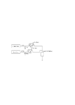
I have a boost converter that generates 200V and a charge pump that generates -60V. I want two seperate those rails from the load through analog switches.
To limit Vgs to +/-5,5V maximum, i have used Zener diodes and control currents (I1,I2).
Through the control current i want to decide wheter -60V or +200V show up at the load output.

The problem is, the analog switches are not working properly and i don´t understand why.
Here is what it does:

If I2=0A and I1=0A output voltage is going down to -60V
If I2=0A and I1=160uA output voltage is further going down to negative voltage
(It seems, the switch controlled by I1 is always on?)

If I2=100uA and I1=0A the output voltage is going up to 0V
If I2=100uA and I1=160uA the output voltage stays at 0V

Any idea how to solve this problem?
It seems that the switch fed by I2 is switching between on and off, but the switch fed by I1 is always on.

I urgently need your help!!!
 

Attachments

  • Analog Switch Problem.png
    Analog Switch Problem.png
    9.5 KB · Views: 80

Please consider that +200V switch must use a PMOSFET and the -60V a NMOSFET. Control polarity will be respectively different.

Both transistors must be rated for at least 260V (300V) Vds.
 

The DC leakage on the gate of the -60V switch causes the protection diode to conduct? Your need giga ohms of insulation here.
An alternative arrangement would be to connect the two PSUs in series (+200V to -60V) with the junction going to your load. then earthing the "other" end of the relative PSU, put that PSU in circuit. There would be a problem if you wanted to switch rapidly, due to the extra capacitance to earth of the PSUs.
Frank

Sorry, i don´t understand exactly what you mean. Do you have a rough sketch for me please? That would help me a lot. It is really really urgent for me!
Switching is very slow. It is around 100 Hz. So, that should not be the problem.

If you mean to put the load between the outputs of boost converter and charge pump, this is a problem, because the charge pump uses the boost converter as clk signal.
See attached.Analog Switch Problem 2.png
 
Last edited:

The +200V goes to the cathode of the zener, so it is reversed biassed. The -60 V also goes to the cathode of the diode so unless there is absolutely no current flowing the diode will be forward biassed. The gate will then be + .8V wrt the source so the FET is on a bit.
Frank
 

In my experience analog switches want something, somewhere to
provide a suitably low impedance for the leakage currents. The
low-Z may not be (and probably isn't) the switch itself, at least
in the "off" case. But the current will go somewhere, and you'd
best be the one who decides.

I have specifically seen self-referred clamping schemes for
high voltage (only ~30V) that worked fine into a test load but
would go crazy at over 1Megohm Zpin in the off state.
 

I think the original topology can basically work with these modifications:
- Using transistors of correct polarity
- Correcting Z-diode polarity for -60V
- Placing resistors in parallel to the Z-diodes
 

I think the original topology can basically work with these modifications:
- Using transistors of correct polarity
- Correcting Z-diode polarity for -60V
- Placing resistors in parallel to the Z-diodes


Thank you for your help! It feels like i am coming closer to the solution.

I think i did now what you suggested:

1. I replaced a PMOS through NMOS transistor for the negative voltage rail.
2. I twisted the Zener diode at the Vgs of the NMOS
3. I added parallel resistors to the Zeners and made a resistor sweep.
This is the new circuit with changes:

Analog Switch Problem Circuit Änderung.png

It seems it works in general, but the only problem is that the output voltage is very much limited. With 100k resistors i can reach: -13V/+100V
 

The polarity of control currents must be different, too. Sinking the current to ground is the correct polarity for both switches.
 

The polarity of control currents must be different, too. Sinking the current to ground is the correct polarity for both switches.

Hi,

i have now changed the polarity of the currents, i made sweeps for resistance, capacitance and current but nothing really helps getting the neccessary voltage levels.

Any idea?
 

i have now changed the polarity of the currents, i made sweeps for resistance, capacitance and current but nothing really helps getting the neccessary voltage levels.
That's about no information without knowing the actual voltage levels and the control circuit. In addition, you should mention the transistor types.
 

That's about no information without knowing the actual voltage levels and the control circuit. In addition, you should mention the transistor types.


At the Moment the circuit with analog Switches at the Output reaches -18V/+100V after 1ms.

The current control circuit for the analog switches is an ideal current source.
The whole System is not regulated yet.

Transistor types are PHC2300N/PHC2300P
 

I believe the transistors should work. But what does "ideal current source" mean, are you talking about a simulation?
 

I believe the transistors should work. But what does "ideal current source" mean, are you talking about a simulation?

Yes. I simulate with Cadence/Spectre.
It is an integrated circuit. I first tried to integrate the switches but it seems the leakage of those transistors is too high.
Then i tried the external Mosfets PHC2300 and it works, but the output voltage is strongly limited. I guess it is a problem of the transistors in combination with very low output current (load is 10nF/5MOhm) but is am not sure.

I need any solution to overcome this problem. Any output switch that works here, as small as possible!
 

Reviewing the simulation results thoroughly will tell you what's the problem.
 

I got it running now with two external NMOS switches. It didn´t work with NMOS and PMOS because the external PMOS had to high Rds,on.

Now i try to integrate it with PMOS transistors. It almost works, but the output voltage starts at -50V instead of 0. I don´t understand why.

PMOS Analog Switches.png
 

You'll need a bipolar output voltage range for the control current driver of the flipped NMOS.
 

You'll need a bipolar output voltage range for the control current driver of the flipped NMOS.

There is no flipped NMOS. Only integrated PMOS.

Can it be a problem of Charge injection maybe?
 

O.K. I see, all PMOS. It's still simulation only? So you can easily "measure" why the problem occurs.
 

O.K. I see, all PMOS. It's still simulation only? So you can easily "measure" why the problem occurs.

Yes, still simulation. Well, its not so easy to measure why it occurs.
I realize, when i make the transistor bigger to decrease the Rds,on the behavior is getting worse. So i can guess that it is not a matter of Rds,on but maybe a matter of Cds ?! When i decrease the control current 1 to 10uA and control current 2 to 100uA it shows best behavior....so probably it is a matter of charge injection?
 

Status
Not open for further replies.

Similar threads

Part and Inventory Search

Welcome to EDABoard.com

Sponsor

Back
Top