Continue to Site

Welcome to EDAboard.com

Welcome to our site! EDAboard.com is an international Electronics Discussion Forum focused on EDA software, circuits, schematics, books, theory, papers, asic, pld, 8051, DSP, Network, RF, Analog Design, PCB, Service Manuals... and a whole lot more! To participate you need to register. Registration is free. Click here to register now.

Problem in timing diagram of Pedroni's FSM book

Status
Not open for further replies.

hobbyiclearner

Full Member level 2
Joined
Oct 27, 2014
Messages
142
Helped
2
Reputation
4
Reaction score
2
Trophy points
18
Activity points
1,296
Hi,

I was going through Pedroni's FSM book and came across pulse detection circuit in Chap 2. As per fig 2.9 (b), if a pulse of greater length than one clock pulse (CP) is given to the ckt of fig 2.10, it is truncated to a length of exactly to a pulse of 1 CP duration which is available (as per the book) in between the input pulse edges. But as per my understanding, it should be available after 1 clock edge. Where am I going wrong pls.?

I am attaching the pdf of the relevant pages from the book and the timing diagram as per my understanding. Pls. see where I am going wrong.

Thanks and Regards,

Hobbyiclearner
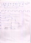
hand_diagram.jpgView attachment pedroni_chap_2.pdf
 

You I/P input is drawn wrong, the rst is active starting on a clock edge so the I/P should be reset shortly after a clock edge instead you seem to have lined it up arbitrarily.

Maybe you misinterpreted the book, because the rest of the waveforms look correct in terms of when the rising edges occur and the output would pulse like you drew starting at the rising edge of Q3 and ending at the rising edge of Q4.

- - - Updated - - -

Just checked the link to the relevant pages of the book and nowhere in the text does it mention that location of the output pulse on a timing diagram.
 

You I/P input is drawn wrong, the rst is active starting on a clock edge so the I/P should be reset shortly after a clock edge instead you seem to have lined it up arbitrarily.

.

Request you to re-check with signal 'inp' of 2.9(b). It starts just before the third rising edge of 'clk' and falls after fourth rising edge of 'clk' ie. it becomes high before a rising edge of clk pulse and falls after the subsequent rising edge of the clk pulse. So the input pulse is greater than one clk pulse. (Instead of third and fourth rising edges of clk, I took second and third. Maybe this should not make a difference,; as per the book the output should be a high pulse of exactly one clk cycle timed in between the input cycle )

Just checked the link to the relevant pages of the book and nowhere in the text does it mention that location of the output pulse on a timing diagram.

Requesting a recheck on page 28 of extract (fig 2.9(b)) where signal 'outp' is given in wave forms as in between the 'inp' pulse. I am not getting the output pulse in between the input pulse. Just for clarification, as per the book, if the pulse is more than 1 clk pulse width it will reduce it to of exactly one pulse width. Though I am getting the correct size of the pulse, I am not able to get the correct timing, ie. the output pulse is not coming in between the edges of the input pulse.

Thanks and Regards,
Hobbyiclearner.
 

You keep referring back to the figure 2.9(b), which is not the timing diagram of figure 2.10.

Figure 2.10 shows a circuit that can perform the function describe by the waveforms shown in figure 2.9(b).

Perhaps you need to go back and reread those pages carefully. I rechecked them and came back with the same conclusion, you are misinterpreting the book.
 

Status
Not open for further replies.

Part and Inventory Search

Welcome to EDABoard.com

Sponsor

Back
Top