Hawaslsh
Full Member level 3
- Joined
- Mar 13, 2015
- Messages
- 167
- Helped
- 5
- Reputation
- 10
- Reaction score
- 7
- Trophy points
- 1,298
- Location
- Washington DC, USA
- Activity points
- 3,461
Hello all,

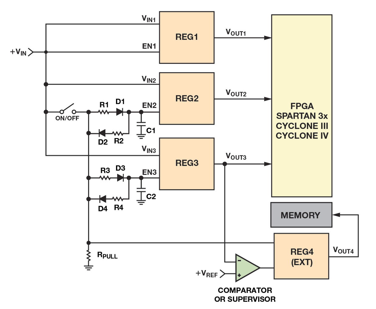
I am trying to implement a simple power supply sequencing that I saw on an ADI article. The picture above shows what I am trying to recreate. My timing requirements aren't strict, I simply need my positive rails turn on before any negative rail and the negative rails to turn off before the positive. So a simple RC time delay on the regulators' enable pins should be enough.
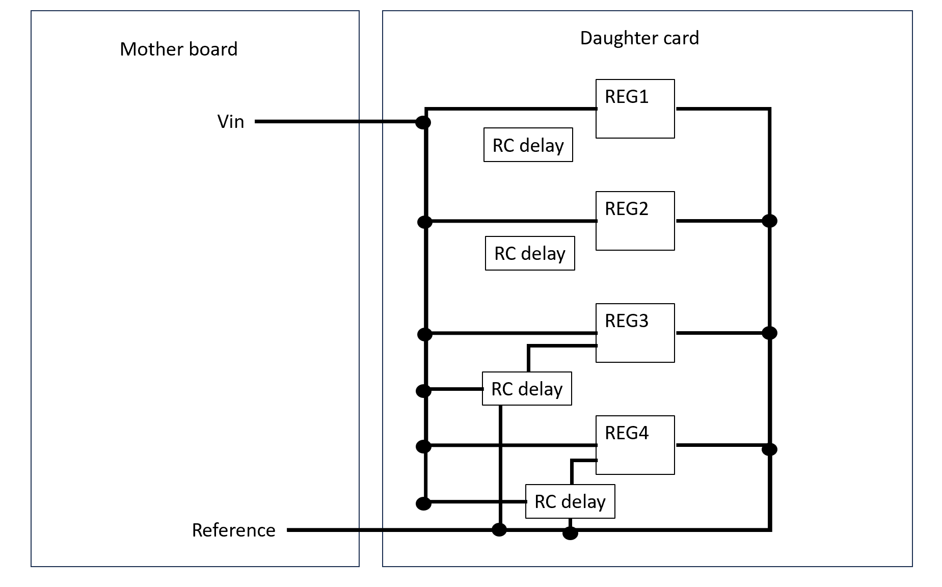
However, my situation is a bit different than the picture above. I do not have a switch to energize / de-energize the RC time delays. I have a daughter board plugging into mother board. The physical connection to the motherboard energizes or de-energizes the board. The power on sequence makes sense. However, I am not entire sure what happens when I unplug the daughter board. (Referenceing the diagram above) When the switch is opened C1 and C2 are discarged through D2, R2, D4, R4 back to the return path. In my case, when I discconect the daugter board, technicly i remove the return path for that discharge current. Am I overthinking this problem, or will removing that return path cause issues? I'm going to go try it on a bread board, but my gut is telling me that charge has no where to go.

Thanks in advance
Sami
I am trying to implement a simple power supply sequencing that I saw on an ADI article. The picture above shows what I am trying to recreate. My timing requirements aren't strict, I simply need my positive rails turn on before any negative rail and the negative rails to turn off before the positive. So a simple RC time delay on the regulators' enable pins should be enough.
However, my situation is a bit different than the picture above. I do not have a switch to energize / de-energize the RC time delays. I have a daughter board plugging into mother board. The physical connection to the motherboard energizes or de-energizes the board. The power on sequence makes sense. However, I am not entire sure what happens when I unplug the daughter board. (Referenceing the diagram above) When the switch is opened C1 and C2 are discarged through D2, R2, D4, R4 back to the return path. In my case, when I discconect the daugter board, technicly i remove the return path for that discharge current. Am I overthinking this problem, or will removing that return path cause issues? I'm going to go try it on a bread board, but my gut is telling me that charge has no where to go.
Thanks in advance
Sami