moisiad
Member level 4
Hi
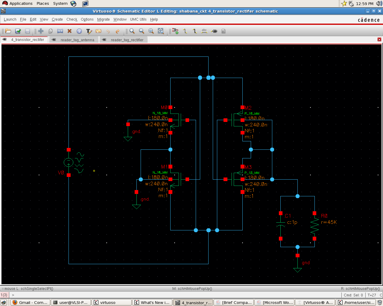
I have designed an active bridge rectifier (see attached figure), with an active (PMOS) diode in the output controlled from a comparator, to generate a DC voltage. The circuit rectifies an AC input signal (1.5Vp) and generates 1.4V in the output
My question is related to the calculation of the power efficiency (n=Pout/Pin) of the rectifier :
The output power is Pout=Vdc(out)/Rload, which is quite straightforward.
To evaluate the input power i use the formula Pin=rms(Iin(t)*Vin(t)). In this case what should be the Iin(t) and Vin(t): the differential I and V waveforms between the two terminals of the input voltage source, or the I and V waveforms from one terminal of the source (The voltage source is floating, no gnd). In the first case (differential) my efficiency is something like 45%, and i wonder where the rest of the power is dissipated.
I would appreciate any feedback regarding the proper power calculation and also if you have any typical values regarding the power efficiency of the specific circuit.
Thanks