Continue to Site

Welcome to EDAboard.com

Welcome to our site! EDAboard.com is an international Electronics Discussion Forum focused on EDA software, circuits, schematics, books, theory, papers, asic, pld, 8051, DSP, Network, RF, Analog Design, PCB, Service Manuals... and a whole lot more! To participate you need to register. Registration is free. Click here to register now.

Possible for a Class C Cascode power amplifier

Status
Not open for further replies.

natnoraa

Full Member level 1
Full Member level 1
Joined
Jun 19, 2011
Messages
98
Helped
12
Reputation
24
Reaction score
11
Trophy points
1,288
Visit site
Activity points
2,108
Possibility of a Class C Cascode power amplifier

Hi,

Would like some advice on a cascode Class C power amplifier. Having ran simulations for a couple of days, I am unable to successfully simulate a cascode Class C Power Amplifier. I would like the bottom transistor to operate as a true class C with Vg < Vth while the top transistor operating at saturation with Vds > Vgs -Vth. However, no matter how I bias the Vg of the top transistor, it's always in triode region. Does anyone know of any way or the possibility of this?

Natnoraa
 

Why your cascode transistor alway in triode? Do you have small vdd voltage?
I think that there are several solutions:
1. Make Vdd higher;
2. Make Vod smaller (~sqrt(2I/K) )
3. Use inductor in load - output dc point = vdd
 

Hi Sarge,

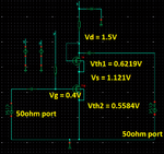
Thank you for your reply. Vdd is 1.5V. Typical Vdd for a single transistor is 1.2V. So for a cascode 1.5V should work. The gate voltage bias for the top transistor is diode connected to its drain. The gate voltage for the bottom transistor is 0.3V (Vth is about 0.55V).

Source voltage of the top transistor (which is the drain voltage of the bottom transistor) turns out to be about 1V. This sets the top transistor to be in triode. No matter how i change the gate biasing voltage for the top transistor (diode connected 1.5V to as low as 0.8V) the source voltage changes accordingly and still forces the top transistor to be in triode (a.k.a region 3 in cadence spectre)
Am working at VERY high frequency by the way. millimeter-wave

Could there be anything else I am doing wrongly from a simple cascoding?

Natnoraa

- - - Updated - - -

I have attached a screenshot for reference :)

Untitled.png

The results are given to me from DC operating point simulation in cadence spectre

- - - Updated - - -

I am able to force top transistor into saturation (region 2) and bottom transistor into linear (region 3) by pushing the Vdd to >3.7V but that's insane for a 65nm process. Moreover, there was a paper published with 1.5V vdd supply using a smaller transistor size on a different 65nm process which claimed it can reach a class c operation. which i think could be not true.
 
Last edited:

Ok, but from your dc point result i don't see a triode region, this is cutoff, Vgs < Vth.
Why do you connect bulk of T6 to it source? Do you want make overdrive voltage smaller with it?

And such kits usually has a special lvt models for transistor.
 

Hi,

Sorry it's my mistake. Region 3 is subthreshold. and yes, I would like Vgs < Vth (for the bottom transistor) for a Class C power amplifier operation.

I'm connecting Vb6 to Vs6 to negate body effect.

I'm only limited to using a nfet_rf model as the PAE is hard to meet. plus the power gain etc.

Natnoraa
 

I forget that there are C class power amplifier.
You show dc points directly in off state, where very low current must flows.
Could you show transient waveforms for cascode transistor?
 

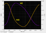
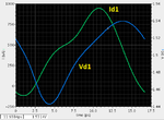
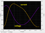
The images for the top and bottom transistors respectively. I ran PSS at -6dBm and the current and voltage waveforms vs time.

The current doesn't peak at where the voltage is at the minimum and it even stores energy (-ve current swing)

bottom xtor.pngtop xtor.png

Natnoraa
 

My assumtion: You have a very small vgs => you must plase Vs of T6 lower.
Ways for it: making width of T6 lower (Vds ~ 1/K) or increasing curent (Vds ~ I)

PS. For complete class C and pure sinusoidal output waveform you also need a harmonic filter as i know.
 

Hi,

I will try your advice again of reducing the W of the top transistor but actually I've done it and still the overall PAE was bad (like -ve because the gain doesn't even hit positive due to both transistor in subthreshold state).

The transmission line at the drain and gate will reject the fundamental frequency and short all other harmonics to AC ground.
Thanks for your help

Natnoraa
 

Oh it is transmission line, i thinked that is just inductor.

One more thing: could you try not diode connection load, but make for it constant dc bias or just place RC filter from output to gate of cascode transistor.

For diode-connected load gain approximately equal to unity.
 
Last edited:

Hi,

It is a rfline model with inductance value. I have ran small signal S-parameters and they showed a good S11 and S21 for the frequency of interest.

I have tried to bias the gate of the top transistor with a separate dc source with voltages swept from 0.8V to 1.2V but to no avail. It's just not easy for a junior engineer researcher like me.

Thanks for the help thus far sarge!

Natnoraa
 

Hi again :)

I wonder about your good result for s-param analysis. With low power level of input signal (small signal analysis) the bottom transistor doesn't go out from subthreshold...
How did you get good s21 (for power gain best choise is gt db10 i think)?

Next thing that i'll do - reducing of vth T6.
 

Hi,

Thanks for the insight of your technical expertise

The S parameter analysis was done with two ports and the rfline as the DUT. one end to serve as a 50ohm port and the other an 1a (acto) ohm resistance (rf ground). could it be wrong? S11 is about -0.2dB which shows high reflection of the frequency of interest and that it doesn't pass through the rfline because S21 is close to -20dB as well. This was how i determined that the rfline could be used as a RFchoke (and filtering out harmonics). I did get not bad results with a single stage transistor for class A.

However, Class AB/C BY RIGHT should yield a higher PAE but am getting only 20%+ which is lower than my class A at close to 30% PAE before matching, which is so wrong. As I explained in an earlier thread, the gain roll-off is at about 30GHz from the foundries' pdk manual. thus the gain isn't sufficient at class AB/C biasing conditions at my frequency of interest sadly. That's why am going into cascode for class C to boost the gain to see how it is

hmmm reducing the Vth of T6 could be an option. I'll look into biasing the body to reduce it since I have a constraint of using only the nfet_rf model. damn. analog electronics back to haunt me again

Natnoraa
 

What type of modulation will you use? May be class E will better solution than C?
 

Hi Sarge,

Cadence spectre (i think) doesn't support a full simulation with modulation schemes (if it does i guess would be OFDM). i'm running simulations based on just sweeping input power and getting results such as psat, op1db, power gain and pae for research publications. am actually needing class c for a specific power amplfier architecture at my frequency of interest. need to make sure class c does not work first before moving on to switching amplifiers :)

Natnoraa

- - - Updated - - -

damn i just realized that the formula, Vt0 is the lowest it can go when i short source and bulk together. i can't body bias to reduce it. am trying smaller transistors. oh well...

formula.png
 

You can simulate it with tran and pss and write modulator on verilogA for example...
But i asked it because i want to know why not use switching amplifier if you need a good efficiency. For OFDM i think building of switching amplifier will quite difficult :)

- - - Updated - - -

damn i just realized that the formula, Vt0 is the lowest it can go when i short source and bulk together. i can't body bias to reduce it. am trying smaller transistors. oh well...

View attachment 101910

I forget it too :)
Ok, did you try to make T6 smaller with constant dc bias? Could you show wafeforms in that case?
 

Hi,

I will take note that it is indeed possible to simulate with a modulation scheme using verilog although at this point of time I am still unsure on how to. will read and figure it out

the architecture am researching on provides rather good linearity and enhanced efficiency even at back off. so i need BOTH linear amplifier (class A and AB) and non-linear amp (class C)

Natnoraa

- - - Updated - - -

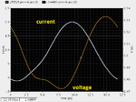
this is the top transistor before and after reducing the size of it from 80um to 40um (width). length is 60nm

before:top xtor.png
after:top xtor2.png

this is the bottom transistor before and after

before:bottom xtor.png
after:btm xtor2.png

- - - Updated - - -

i have also separately bias the gate voltage for the top transistor from 1.5V to 1.2V. Vdd is still 1.5V

- - - Updated - - -

from what i have observed, the class C just does not work very well at my frequency of interest. at 5GHz, i ran a simulation and the waveform is almost perfect; conduction angle <180 degree. but this simulation shows the class c doesn't turn off properly and fast enough. bummer
 

Hi,

I will take note that it is indeed possible to simulate with a modulation scheme using verilog although at this point of time I am still unsure on how to. will read and figure it out

Not verilog, verilogA

from what i have observed, the class C just does not work very well at my frequency of interest.

This was my next surmise... Well, good luck in your research, it will be quite good if you'll post here working result for such frequency.
 
Hi,

oops, verilogA. will note this down for future reference.

Really thanks for the help and insight provided. Yep, only one working class C power amplifier publication at this frequency so far but i highly doubt the results as its drain efficiency reported was way lower than my class A's PAE which is very not helpful and dubious.

will come back here someday if successfully demonstrate it. Thanks again!

natnoraa

- - - Updated - - -

Hi again,

May I also ask a question?

Power Gain,PAE and OP1dB if i simulate BEFORE doing input/output matching, what are the differences? Is it accurate or should i just say that's the maximum raw results I can get after matching network?

Natnoraa
 

Hi,

Thanks for the insight of your technical expertise

The S parameter analysis was done with two ports and the rfline as the DUT. one end to serve as a 50ohm port and the other an 1a (acto) ohm resistance (rf ground). could it be wrong? S11 is about -0.2dB which shows high reflection of the frequency of interest and that it doesn't pass through the rfline because S21 is close to -20dB as well. This was how i determined that the rfline could be used as a RFchoke (and filtering out harmonics). I did get not bad results with a single stage transistor for class A.

However, Class AB/C BY RIGHT should yield a higher PAE but am getting only 20%+ which is lower than my class A at close to 30% PAE before matching, which is so wrong. As I explained in an earlier thread, the gain roll-off is at about 30GHz from the foundries' pdk manual. thus the gain isn't sufficient at class AB/C biasing conditions at my frequency of interest sadly. That's why am going into cascode for class C to boost the gain to see how it is
Why do you think a cascode would increase the gain of a class C amp? It will probably have better isolation, but not better gain. It will certainly hurt efficiency, especially with such a low Vdd.

It sounds like you're trying to rush a concept before understanding some of the basics. You should go back and get a simple class C working, perhaps at a much lower frequency (or with much smaller FETs), just so you can familiarize yourself with them. Then you can try adding in novel stuff like cascodes.
 

Status
Not open for further replies.

Similar threads

Part and Inventory Search

Welcome to EDABoard.com

Sponsor

Back
Top