jayeffe
Junior Member level 2
Hello everyone . I am trying to insert the pins into the ADDA terasic board. But I'm having a little trouble. I have currently followed the guide and found a few things.
As the example uses channel B, it puts the pin on PLL of JP1.
Then on JP5. (in verilog I have a module that deals with the PLL).
I have tried and it works.
I also wanted to do the same thing to enable channel A.
I then put the pins on PLL, referring to AD channel A.
JP2 JP4.
I am interested in knowing if it is okay and above all if the position 1-2 is that. In the manual the card is reversed and I got confused.
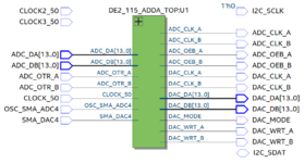
This is the demo code, top level only
the didactic project asks me to perform the loop following the example given in the manual.
I tried to do the same thing with channel A.
So DAC_DA I connected it to ADC DA.
Because of how this code is done I get a different signal from Channel B.
the schematic reports that DAC_DA and DAC_DB are the same signal. so creating the loop I should have the same output signal.
As the example uses channel B, it puts the pin on PLL of JP1.
Then on JP5. (in verilog I have a module that deals with the PLL).
I have tried and it works.
I also wanted to do the same thing to enable channel A.
I then put the pins on PLL, referring to AD channel A.
JP2 JP4.
I am interested in knowing if it is okay and above all if the position 1-2 is that. In the manual the card is reversed and I got confused.
This is the demo code, top level only
Code:
module DE2_115_ADDA_TOP(
                        CLOCK_50,
                        ADC_CLK_A,
						ADC_CLK_B,
						ADC_DA,
						ADC_DB,
						ADC_OEB_A,
						ADC_OEB_B,
						ADC_OTR_A,
						ADC_OTR_B,
						DAC_CLK_A,
						DAC_CLK_B,
						DAC_DA,
						DAC_DB,
						DAC_MODE,
						DAC_WRT_A,
						DAC_WRT_B,
						OSC_SMA_ADC4,
						SMA_DAC4
                        );


input		          		CLOCK_50;

output		          		ADC_CLK_A;
output		          		ADC_CLK_B;
input		    [13:0]		ADC_DA;
input		    [13:0]		ADC_DB;
output		          		ADC_OEB_A;
output		          		ADC_OEB_B;
input		          		ADC_OTR_A;
input		          		ADC_OTR_B;
output		          		DAC_CLK_A;
output		          		DAC_CLK_B;
output		    [13:0]		DAC_DA;
output		    [13:0]		DAC_DB;
output		          		DAC_MODE;
output		          		DAC_WRT_A;
output		          		DAC_WRT_B;
input		          		OSC_SMA_ADC4;
input		          		SMA_DAC4;

//=======================================================
//  REG/WIRE declarations
//=======================================================
assign  DAC_WRT_B = CLK_125;      //Input write signal for PORT B
assign  DAC_WRT_A = CLK_125;      //Input write signal for PORT A

assign  DAC_MODE = 1; 		      //Mode Select. 1 = dual port, 0 = interleaved.

assign  DAC_CLK_B = CLK_125; 	  //PLL Clock to DAC_B
assign  DAC_CLK_A = CLK_125; 	  //PLL Clock to DAC_A

assign  ADC_CLK_B = CLK_65;  	  //PLL Clock to ADC_B
assign  ADC_CLK_A = CLK_65;  	  //PLL Clock to ADC_A


assign  ADC_OEB_A = 0; 		  	  //ADC_OEA
assign  ADC_OEB_B = 0; 			  //ADC_OEB

/////////////////////////////////////

wire    [13:0]	sin10_out;
wire    [13:0]	sin_out;

wire    [13:0]	comb;


wire    [31:0]	phasinc1;
wire    [31:0]	phasinc2;

wire    g = 0;
wire    v = 1;

assign  phasinc1 = {g,g,g,g,v,v,g,g,v,v,g,g,v,v,g,g,v,v,g,g,v,v,g,g,v,v,g,g,v,v,g,v};
assign  phasinc2 = {g,v,g,g,g,g,g,g,g,g,g,g,g,g,g,g,g,g,g,g,g,g,g,g,g,g,g,g,g,g,g,g};

assign  DAC_DA = comb; //B
assign  DAC_DB = comb; //A


//=======================================================
//  Structural coding
//=======================================================

nco91 sin1    (
				  .phi_inc_i(phasinc1),
			      .clk	    (CLK_125),
				  .reset_n  (v),
				  .clken	(v),
				  .fsin_o	(sin_out),
				  .fcos_o   (),
				  .out_valid(ovalid)
		       );

nco91 sin2      (
				  .phi_inc_i(phasinc2),
				  .clk	    (CLK_125),
				  .reset_n  (v),
				  .clken	(v),
			      .fsin_o	(sin10_out),
				  .fcos_o	(),
			      .out_valid(ovalid)
		       );


pll  pll_100   (
				 .inclk0(CLOCK_50),
                 .pllena(v),
                 .areset(g),
                 .c0    (CLK_125),
                 .c1	(CLK_65)
			   );

lpm_add    lpm  (
                 .clock (CLK_125),
                 .dataa ({g,~sin_out[12],sin_out[11:0]}),
                 .datab ({g,~sin10_out[12],sin10_out[11:0]}),
                 .result(comb)
                );

endmodule
the didactic project asks me to perform the loop following the example given in the manual.
I tried to do the same thing with channel A.
So DAC_DA I connected it to ADC DA.
Because of how this code is done I get a different signal from Channel B.
the schematic reports that DAC_DA and DAC_DB are the same signal. so creating the loop I should have the same output signal.
Attachments
Last edited: