K33rg4t3
Full Member level 3
Hey
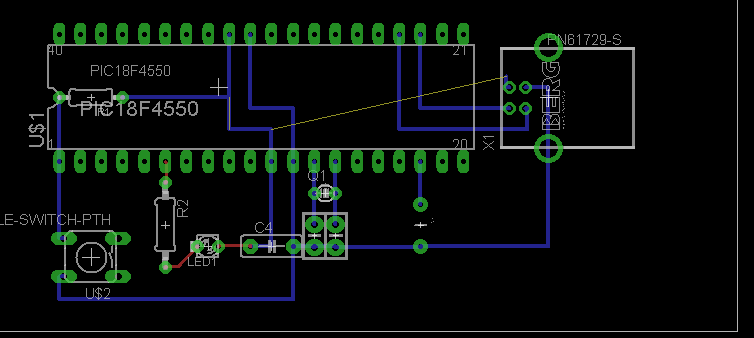
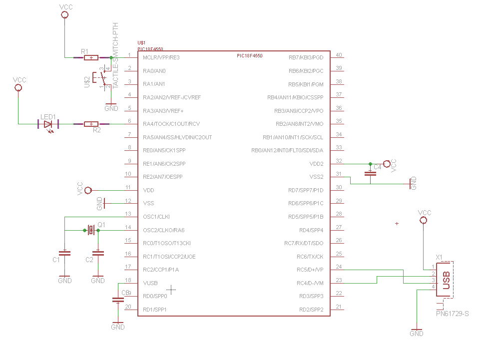
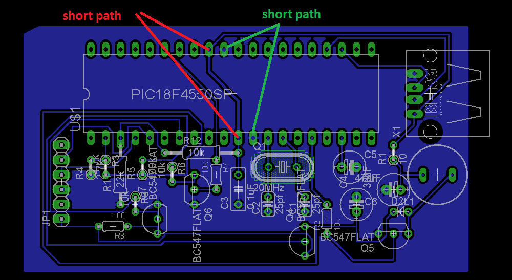
I want to design PCB for my PIC18F4550 board.
But this part is not available in Eagle.
How to add it?
I've found: https://github.com/chiengineer/Eagle-Libraries
But I don't know where to put those files after downloads??
Thanks in adavance
I want to design PCB for my PIC18F4550 board.
But this part is not available in Eagle.
How to add it?
I've found: https://github.com/chiengineer/Eagle-Libraries
But I don't know where to put those files after downloads??
Thanks in adavance