Continue to Site

Welcome to EDAboard.com

Welcome to our site! EDAboard.com is an international Electronics Discussion Forum focused on EDA software, circuits, schematics, books, theory, papers, asic, pld, 8051, DSP, Network, RF, Analog Design, PCB, Service Manuals... and a whole lot more! To participate you need to register. Registration is free. Click here to register now.

Photodiode amplifier

Status
Not open for further replies.

umery2k75

Advanced Member level 1
Joined
Apr 19, 2006
Messages
434
Helped
41
Reputation
80
Reaction score
15
Trophy points
1,298
Location
Pakistan
Activity points
5,748
Hello everyone,
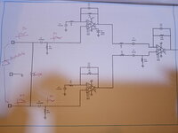
This is the actual circuit made on a PCB and I couldn't get any stable results out from this circuit I injected Sin wave on the input of this amplifier instead of photodiode and I experiment with different frequency from 20Hz all the way to 1Khz Vpp 20mV to 1Vpp, but I couldn't get any meaning full result out from this. I really doubt if this is a proper engineering done, because transconductance amplifier are being used either in photovoltaic mode or photoconducive mode. Please shed some light on it.
 

Attachments

  • 16752059166675411277647766107203.jpg
    16752059166675411277647766107203.jpg
    2.6 MB · Views: 103

You surely determined gain, corner frequencies and maximal undistorted output magnitude before performing the tests?
--- Updated ---

The other question is, why did you select a voltage amplifier with differential input for photo diode and not e.g. a single ended transconductance amplifier?
 

Hi,

Never seen this kind of amplifier used with a photodiode.
The photodiode operates in "photovoltaic" mode, thus has poor linearity.

To debug: I'd use a scope and trace U1 output and U2 output.

Btw: "couldn't get meaningful output" is useless information, we have no idea what this means.

Klaus
Hello Klaus and everyone else,
I explain what I mean by meaningful output. I means the output is with noise and with fluctuation and no proper sense can be made by looking at the oscilloscope output at the last opamp. It amplifies no difference. Until I short the function generator ground with the circuit ground, otherwise there is no sense one can draw. But in real circuit photodiode is completely isolated with circuit ground. So function generator ground must not be short with circuit ground. I am using function generator as a simulating signal in place of photodiode . You can watch the

Experiments video difference amplifier


I made this circuit on varioboard and injected 1Vpp sine wave across 15k reaistor where photodiode needs to be connected and light is fallen on the photodiode like sine wave shadows, so output should be like a modulated sine wave. So I made same circuit.

This circuit is actually used by a manufacturer in their photo diode amplifier design and I really doubt if they are engineered properly because later I came to know about their bad reputation in their product engineering design and on my recommendation, my different customers purchased their equipment and other products from them, few other products never worked for the single time although they were powered up and this product has issues. Majority of the time this unit do not work properly. The manufacturer never responds on any technical matter but Is open to discuss new sales and I have to fix their design because I cannot make my custom unhappy.
 
Last edited:

Hi,

in this case I´d not blame it on the original manufacturer.

I see a lot of possible issues in the video:
* no proper PCB with solid GND plane
* missing GND wiring concept
* signal generator (mains powered?) - not connected to a circuit_GND star point
* power supply (mains powered?) - not connected to a circuit_GND star point
* scope (mains powered?) - not connected to a circuit_GND star point
* circuit is meant for a high impedance floating photodiode.

So I guess the mains powered devices introduce a lot of noise into the signals.

--> you need to connect all the devices to a common circuit_GND star point.

and - as already mentioned - show us a scope picture of the U1 and U2 outputs.

Klaus
 

Are you excluding ambient light sources (full of 120Hz hum,
are overhead fluorescent lights' EMI -and- light output)?
What's your "dark box" look like?

A voltage mode op amp with a feedback resistor will make
you an OTA (well, actually a transimpedance amplifier, not
a transconductance amplifier). But you had best look at the
realities of signal range and supply.

You will have a better (linear w/ input power) result from
amplifying photocurrent (your "photoconductive", though
different from the conductivity modulation of a CdS or other
no-junction element). On the other hand a log response
(as photovoltaic mode) might suit some interests such as
dynamic range mattering more than great accuracy.
 

Hi,

I think the OP currently does not use a photodiode.

***
from the design I think the capacitors C7, C8 are no good idea, because C7 sees (low impedance) 1k + virtual_GND while C8 sees 1k + 100k. If I´m not mistaken then this causes two different cutoff frequencies, which kills common mode suppresion of the difference amplifier.

Klaus
 

Status
Not open for further replies.

Similar threads

Part and Inventory Search

Welcome to EDABoard.com

Sponsor

Back
Top