Continue to Site

Welcome to EDAboard.com

Welcome to our site! EDAboard.com is an international Electronics Discussion Forum focused on EDA software, circuits, schematics, books, theory, papers, asic, pld, 8051, DSP, Network, RF, Analog Design, PCB, Service Manuals... and a whole lot more! To participate you need to register. Registration is free. Click here to register now.

Phase Shift or Polarity Inversion for Push-Pull Configuration??

Status
Not open for further replies.

pYrana13

Junior Member level 1
Joined
Nov 29, 2009
Messages
16
Helped
0
Reputation
0
Reaction score
0
Trophy points
1,281
Activity points
1,407
Hi all,

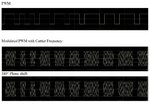
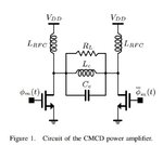
In Class-D amplifier, the transistors are in Push-Pull configuration. To drive the transistors using the PWM signal, the signal given at either transistor is inverted of the other signal.

The question is:
From most of the references I read, why they normally used 180 degree phase shift?? If PWM phase is shifted, it is not exactly inverted. Thus both signals which drive the transistors are not inverted to each other, but only delay.

Could somebody explain this to me. TQ.
 

The carrier frequency of the PWM in a class-D amplifier has only one frequency. PWM changes its duty-cycle not its frequency.
Then the signal inversion can be done with a 180 degree phase shift which produces a delay.
 
The signals are basically inverted, but with a short asymmetrical delay to operate the switches break-before-make.
 

The carrier frequency of the PWM in a class-D amplifier has only one frequency. PWM changes its duty-cycle not its frequency.
Then the signal inversion can be done with a 180 degree phase shift which produces a delay.

So does it mean the transistors will be driven by both signals, which are product of modulation with carrier frequency and its phase-shifted signal(inverted signal) as shown below? Is it right?
 

Attachments

  • PWM and modulated signal.JPG
    PWM and modulated signal.JPG
    204.1 KB · Views: 122

pYrana,
You do not show a PWM carrier. Instead you show a high frequency sinewave carrier that is amplitude-modulated by a rectangular low frequency signal.

PWM is the opposite. It is a high frequency rectangular carrier with the width of its pulses modulated by a low frequency signal.
 

pYrana,
You do not show a PWM carrier. Instead you show a high frequency sinewave carrier that is amplitude-modulated by a rectangular low frequency signal.

PWM is the opposite. It is a high frequency rectangular carrier with the width of its pulses modulated by a low frequency signal.

I'm actually designing a class-D power amplifier (shown in circuit below) using delta sigma modulation as the modulation method. The output signal(PPM) which should be fed to both transistors, is similar to PWM, as shown by the image below.

So i have this PPM. The question is why most references/reports I read said that both transistors operate as switches driven by a square wave 180 degrees out of phase, which I think is not exactly inverted. If I just made a 180 degree phase shift for the signal below(PPM), what is the expected result? Is it inverted or is it delayed?

I tried and got delayed signal, which is not a complimentary signals which can drive transistors in push-pull configuration. Or do I really need to modulate PPM with carrier frequency first, like my post before?
 

Attachments

  • circuit.JPG
    circuit.JPG
    37.4 KB · Views: 84
  • Modulation.JPG
    Modulation.JPG
    181.3 KB · Views: 79

For most purposes the time delay should work. If you consider a PWM signal that is modulated by a low frequency sine wave (typical VFD drive waveform). As the sine wave passes through zero, there will no PWM output at all during the carrier frequency period. Now the sine wave rises a little bit (1% of max?) so a narrow pulse appears. We can use this to drive say the top half of the H bridge amp. What do we use to drive the bottom half?. If we use the "delayed" method then there is no drive. If we invert the narrow pulse, we get the corresponding narrow pulse applied the the lower transistors of the \h bridge so the amp works as expected and delivers a narrow pulse of current, which will be integrated to form a small analogue voltage.
Invert every time!! (but watch out for spurious delays creeping in)
Frank
 

I didn't previously notice the schematic with single ended output transistors in post #6. If nothing is said about the topology and RF PA isn't explicitely stated, I associate a H bridge with class-D amplifier.

The single ended topology has a larger tolerance for different controlling waveforms, it must not necessarily be exactly inverted. Nevertheless, a PWM square wave can be much more easily inverted than delaying it by exactly a half period. Or which delay method did you consider?

So the answer about suitable way to generate the control waveform is obvious in practical sense.

I use rat-race hybrid/coupler to have a 180 degrees phase shift. I give my PPM signal at the input of the coupler, and I get 2 outputs of the same signal that differs by 180 degrees phase. But this doesn't allow only 1 transistor works at a time. The signals can be seen below.
 

Attachments

  • RatRaceOutput.JPG
    RatRaceOutput.JPG
    75.5 KB · Views: 76

Your new waveform in post #6 is PWM. But your circuit will not work because it is a half-bridge that pulls down well but almost nothing pulls up the outputs.
You need a full H-bridge that has push-pull on each output. You also need some "dead time" to allow an upper or lower half of the H-bridge to turn off before the other half turns on to avoid a "shoot-through" current.

You have a high impedance parallel LC resonance parallel to the low impedance speaker that will not work. Instead each end of the speaker needs a lowpass series LC filter.

Instead of us telling you what is wrong, please study and understand a class-D amplifier circuit.
The "current mode" class-D circuit shown in post #6 hasn't to do with a class-D topology used for low frequency (e.g. audio) amplifiers. It's a RF power amplifier concept and isn't normally used with PWM control. As you can imgaine, the real gate and drain voltages aren't square waves.

I'm not sure if the OP is aware of the differences between CMDC and regular class-D amplifiers. The references to PWM suggest he isn't.

P.S.: You can (in principle) operate a transformer based push-pull audio amplifier in class-D PWM mode. Nobody would do this because it involves a quite large transformer. Although the topology would be similar to the post #6 schematic, you won't designate it current mode class-D.
 
Last edited:

Status
Not open for further replies.

Similar threads

Part and Inventory Search

Welcome to EDABoard.com

Sponsor

Back
Top