sabu31
Advanced Member level 1
Dear All,
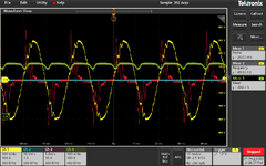
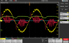
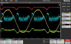
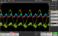
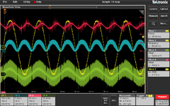
I am experimenting on a PFC circuit using UCC28019. The system turns on after AC input of 125V . And output is around 400V. However, the input current is not correcting. THe load used is 280 Ohms. I am attaching the waveform.
The input current is in Red. The output voltage is in Green. The input voltage is in yellow.
Though I have designed for 2kW.
The current sense resistor used is 0.05Ohms. Is it current sense hitting upper limit.
Please let me know what should be done to troubleshoot the system.
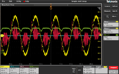
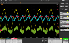