Continue to Site

Welcome to EDAboard.com

Welcome to our site! EDAboard.com is an international Electronics Discussion Forum focused on EDA software, circuits, schematics, books, theory, papers, asic, pld, 8051, DSP, Network, RF, Analog Design, PCB, Service Manuals... and a whole lot more! To participate you need to register. Registration is free. Click here to register now.

PCB Editor: DRC error & via-Shape conn. do not produced. bug or Migration Problem?

Status
Not open for further replies.

valeriogiampa

Member level 3
Member level 3
Joined
Jul 3, 2008
Messages
58
Helped
5
Reputation
10
Reaction score
5
Trophy points
1,288
Location
ITALY
www.linkedin.com
Activity points
1,897
PCB Editor: DRC error & via-Shape conn. do not produced. bug or Migration Problem?

Hi everyone,
I am using Cadence PCB Editor 16.3 to develop a board (4 layers).
I have 3 vias connected to the GND_RF net.
The Top Layer and Inner2 Layer have a plane connected to GND_RF.
The Inner 3 Layer has a solid fill shape connected to the VCC Nets (VCC1 and VCC2).
The bottom has same nets connected to the GND_RF net.
The problem produced by PCB Editor is descripted by this points:
1. The vias are connected to the plane in the top layer (correct), to the net in the bottom layer (correct) but are isolated respect at the plane on inner 2 layer (error becouse the plane and the vias are connected at the same net: GND_RF).
2. In the Inner 3 layer, the Vias are inside at the solid fill plane of the VCC nets but any drc errors are shown by the PCB Editor.
I have 3 hypothesys:
1. the database of the board has an error;
2. the PCB Editor has a bug.
3. The design of the board has started on a Linux version of PCB Editor 16.3, than I have revisioned this board with a Windows version of PCB Editor 16.3. Is it possible that the migration of the board file from Linux to Windows has generated this problems?

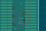
In the attached file you can see the 3 vias in the top, inner2, inner3 and bottom layers.

What is the problem/Bug?
Can anyone suggest me a solution at this bug?

attached files:
https://obrazki.elektroda.pl/8314813900_1361368329.png
https://obrazki.elektroda.pl/4068540400_1361368329.png
https://obrazki.elektroda.pl/7130890300_1361368330.png
https://obrazki.elektroda.pl/4280081500_1361368330.png
 

Attachments

  • bottom.png
    bottom.png
    23.5 KB · Views: 94
  • inner2.png
    inner2.png
    27.8 KB · Views: 98
  • inner3.png
    inner3.png
    57.7 KB · Views: 106
  • top.png
    top.png
    21.4 KB · Views: 91

Re: PCB Editor: DRC error & via-Shape conn. do not produced. bug or Migration Problem

Hi,

Please check what kind of shape you are using. dynamic or static ..? and check the constraint manager via to shape clearance in all layer.(minimum 5 to 8 mils). Tool doesn't had such bug as i know. you have to update database .>> Tool >database check>select both option and check .i think some thing you made mistake in constraint .

Dear praveenlb, The constraints manager is set correctly: The clearance via to shape is configured at 200um. The shapes are: 1) the shape in the inner2 (GND Plane) is "dynamic"; 2) the shape in the inner3 (VCC) is static.
The constraints Manager is set up correctly (200um). Also, There are no DRC waived.
This is only an anomaly: If I copy the VIA that has generated the short in another region I realize that behaves in the same way (no DRC on a static shape and no fill on the dynamics shape connected to the same net).
If I copy another VIA in a position close to this immediately observe the generation of the DRC error on the static shape and the correct fill with the dynamic shape connected to the same net.
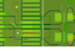
It is difficult to explain this anomaly. For this reason, I have attached to images that shown this to test that I have executed to observe this anomaly: (1) figure 1: I copy the bad VIA in the other point where there is a static shape; (2) I copy an other VIA near in the region where there is a short circuit.
 

Attachments

  • immagine1.png
    immagine1.png
    70.9 KB · Views: 90
  • immagine2.png
    immagine2.png
    78.1 KB · Views: 97

Re: PCB Editor: DRC error & via-Shape conn. do not produced. bug or Migration Problem

Hi,
Use same type of copper in all the layer. if you use one side dynamic copper and another side static copper might be the problem.
static shape you have to update manually .but dynamic shape will be update automatically. while releasing the Gerber you are not able to generate files. it give error massage. understand the concept of dynamic and static copper .

- - - Updated - - -

IF have difficulty send the board file. i will clear that DRC. my version is 16.1 you can down convert if you have higher version
.
 

Re: PCB Editor: DRC error & via-Shape conn. do not produced. bug or Migration Problem

Dear praveenlb.
I think that the description of the problem is not clear.
I know very well how PCB Editor works, the difference between the Static and Dynamic Shape, how the static and dynamic shape work, how the user have to use this object and how the user have to configure tha constraints manager.
The problem is not related at the type of object used or how the user have used it in the design.
The problem is related at this specific point: Why is it the reason that a Via A (padstack name VIA025_015_035 - image1) connected at a net VCC1 and placed into the static shape connected to GND don't produce a DRC, while an other VIA B (padstack name VIA025_015_035 - image2) connected to VCC1 and placed into the static shape connected to GND produce correcly a DRC?
The second question is: Why is it the reason that the Via A (padstack name VIA025_015_035 - image1) connected at a net GND and placed into a dynamic shape plane connected to GND don't produce a connection between the VIA and the plane, while an other VIA B (padstack name VIA025_015_035 - image2) connected to GND and placed into the a dynamic shape place connected to GND produce correcly a connection between the shape and the VIA?
There are:
- an object VIA A that PCB Editor don't use correctly when it is placed into the dynamic or static shape.
- an object VIA B that PCB Editor use correctly when it is placed into the dynamic or static shape.
- The VIA A and the VIA B are two istance of the same padstack componente VIA025_015_035.
-The padstack VIA025_015_035 is defined correctly: pad/antipad/Thermal in the top, bottom and default inner layer + drill dimension: Pad=0.25 - Thermal=0.35 - Antipad=0.35 - DRILL=0.15 - Plated.
I hope this new details make the problem more clear.
 

Re: PCB Editor: DRC error & via-Shape conn. do not produced. bug or Migration Problem

Hi,
I never faced such problem in design.if possible send the board file let me check it out.
 

Status
Not open for further replies.

Part and Inventory Search

Welcome to EDABoard.com

Sponsor

Back
Top