Continue to Site

Welcome to EDAboard.com

Welcome to our site! EDAboard.com is an international Electronics Discussion Forum focused on EDA software, circuits, schematics, books, theory, papers, asic, pld, 8051, DSP, Network, RF, Analog Design, PCB, Service Manuals... and a whole lot more! To participate you need to register. Registration is free. Click here to register now.

Pass transistor in LDO

Status
Not open for further replies.
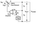
What should be the pass transistor design for optimum design. The Mos should be in CG state or CS or CD. Usually PMOS will be used in CG form .WHat happens if we use in CG or CD
You use the configuration that is appropriate for the circuit function. For the posted regulator design the CS configuration is used (which incidentally will be unstable without an added compensation circuit). Any other configuration would require a redesign of the circuit.
 

Depending on what external resources are available, the
choice of a PMOS pass FET for positive output voltages
becomes less of a "given". It's a no-brainer when VIN
exceeds VOUT or GND by a comfortable margin so you
can get a decent gate overdrive. But if you look at the
POL space where (say) you're making the 0.9V for your
shiny new high speed logic core, from the crusty old 1.5V
already on the board, well, that PMOS pass FET is good
for roughly nothing. Then you see people flipping over to
a NMOS pass FET, common drain, with an AUX feed from
the legacy 3.3V or 5V supplies to run the housekeeping
and provide the over-the-main-rail bias potential.
 

ldo.JPG vin is 2-2.4 v, Vout should be 1.8v. So pass transistor SHould sustain that.And we should look to it the loop gain requirement too. So CS is better than CG right as CS amplifier dominant pole is near than the CG amp
 

Screenshot-2.JPGScreenshot-1.JPG The PMOS pass transistor is not in saturation alll the time. why is it so.The gate input i fed is less than 1.5v. BTW Input to voltage regulator is 2-2.4. output should be 1.8v. so the table i ve attached is the various input voltage and region in which M15 is. Please tell what s been wrong.
 

Your operating point in closed loop depends on the load
current demanded and VIN-LOAD headroom. The Vgs
will be swung to get that current - or peg low and still
fail. But this is the dependent variable, asserted by the
control loop to make the feedback right.

The gate drive from amplifier needs to be rail-rail output
capable to get both minimum leakage / best Iout(min),
and maximum output current / minimum dropout voltage
at low line.

Make it easy on yourself and break this down to its
simplest case - min line, max load, Vgate=GND will
tell you all you need to know about the pass FET
drive; max line, min load, Vgate=VIN will tell you
about leakage (to the extent that your model is
realistic, there).

If you can't make it at these two cases then the rest
of circuit design has nothing for you and you need a
better (could be bigger, could be smaller, could need
better process) pass FET.
 

My load current should be less than 50mA. So what should be the W/L.How high it should be to maintain Pmos in saturation always?
 

When VIN-VLOAD < VT, you have no real chance of the
pass FET being in saturation. You would need a very low
VT device for that, and then you'd have the leakage
problem to deal with (and no means other than wasting
current).

You want VIN-VLOAD as low as 0.2V. Saturation ain't
gonna happen at that corner.
 

Yea and to support 50mA of load current i need PMOS transistor W/L to be very very high. But in 180nm tech. I m working on cadence.So it takes maximum value of width to be 100u.So what do i do. How to increase this width.
 

You want less finger width and more fingers. Too wide
and your gate resistance becomes a factor, along with
the possibility that you can't reliably pull the current
out one end of the stripe, that the channel can deliver.
That's electromigration stuff.

Not to mention power density issues in a maximally-
compacted device (close-in thermal rise, an interesting
problem to model in itself).

If you intend to route power laterally, out the end of
the finger on Met1, then you want to determine the
current density rule and then set # fingers to divide
the output current acceptably among them, and then
put width where it needs to be. If that is still more
than the W limit, use more fingers and quit worrying
about finger current density.

Routing out vertically to thicker metal is also a way
to go; makes you a routing obstacle though, if you
are not the only guy on the chip.
 

Status
Not open for further replies.

Similar threads

Part and Inventory Search

Welcome to EDABoard.com

Sponsor

Back
Top