shockingshockley
Member level 1
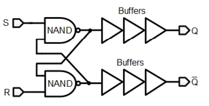
Hello. I am implementing this SR latch circuit below using Verilog:

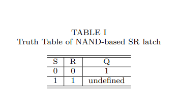
This is the expected logical truth table for this SR latch:

This is the Verilog code I wrote:

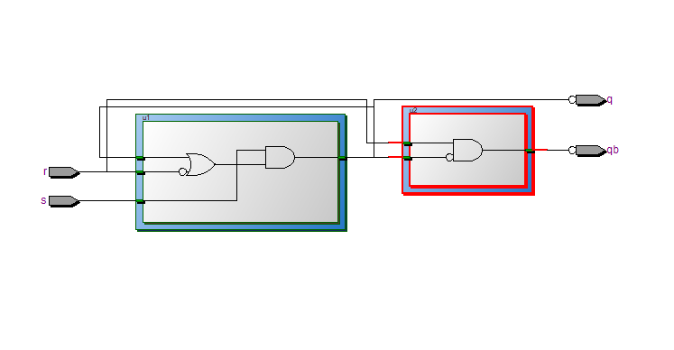
The corresponding technology map is this after I compile the Verilog code. It is not the same as the NAND SR latches.

After compiling, I run the functionality check to observe the input and output waveforms:

However, the output Q is always logic 1 throughout the period. It should have an undefined outputs of 0 and 1. Could you please advise me what is something wrong in my Verilog implementation and behavioral simulation? Thanks in advance.
This is the expected logical truth table for this SR latch:
This is the Verilog code I wrote:
The corresponding technology map is this after I compile the Verilog code. It is not the same as the NAND SR latches.
After compiling, I run the functionality check to observe the input and output waveforms:
However, the output Q is always logic 1 throughout the period. It should have an undefined outputs of 0 and 1. Could you please advise me what is something wrong in my Verilog implementation and behavioral simulation? Thanks in advance.