Continue to Site

Welcome to EDAboard.com

Welcome to our site! EDAboard.com is an international Electronics Discussion Forum focused on EDA software, circuits, schematics, books, theory, papers, asic, pld, 8051, DSP, Network, RF, Analog Design, PCB, Service Manuals... and a whole lot more! To participate you need to register. Registration is free. Click here to register now.

OTA common mode voltage problem

Status
Not open for further replies.

6sbtixjo

Junior Member level 1
Joined
Jan 1, 2012
Messages
18
Helped
0
Reputation
0
Reaction score
0
Trophy points
1,281
Visit site
Activity points
1,430
I am designing a 2 stage Miller compensated OTA. I have problem in fixing the output common mode voltage. There was no problem when i designed a differential output OTA, as a CMFB loop ensured proper output DC voltage. But when i tried to design a single ended OTA, i dont get the desired common mode voltage. The first stage common mode output voltage i got was correct as per my design, but the second stage output common mode voltage i get is 10 mV, while i require a 0.9V output common mode voltage. Is there a way to properly fix the output common mode voltage? Untitled.png
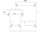
 

Hi, a
Are the current sources & nmos load ratioed properly?
 

yes. i designed the first stage for a current of 100uA and second stage for 340uA. The transitors are sized properly. But still i dont see a way to fix the drain voltage of the second stage. Or for the sake of ease, lets consider a grounded NMOS common source amplifier with a PMOS current source load. How can the drain voltage be fixed? Plz help me.
 

If You have single ended ota an output dc level depends only (assuming no offset voltage) to a feedback configuration - e.g. if your ota works as invert amplifier your output dc level will be equal to reference voltage putted on non-invert input, the same You obtain for source follower configuration, etc.
 

so should i not worry about the common mode voltage at the output in the open loop configuration? Because of this improper value at the output, the nmos in the second stage goes to triode region. so i am unable to check the GBW.. any help on that?
 

OTAs always works in negative closed loop configuration. In open loop its works as comparator.

To simulate open loop behaviour you need an ota in closed loop configuration (e.g. as source follower) which bias ota cell in open loop (not dirtectly by through vcvs) and look for ac response at the output of open loop cell.
If you using spectre You could also simulate one closed loop ota with analogLib/iprobe item which "opening" loop for stb simulation and look for the output. In this way You obtain open loop magnitude and phase response.
 

I am using Cadence Spectre. Can you please tell me how do I check for the open loop magnitude and response after i connect the ota in unity gain configuration. I have not used the iprobe method you mentioned. Please explain.
 

Status
Not open for further replies.

Similar threads

Part and Inventory Search

Welcome to EDABoard.com

Sponsor

Back
Top