Continue to Site

Welcome to EDAboard.com

Welcome to our site! EDAboard.com is an international Electronics Discussion Forum focused on EDA software, circuits, schematics, books, theory, papers, asic, pld, 8051, DSP, Network, RF, Analog Design, PCB, Service Manuals... and a whole lot more! To participate you need to register. Registration is free. Click here to register now.

opamp osciltions problem which didnt show on LTSPICE

yefj

Advanced Member level 4
Joined
Sep 12, 2019
Messages
1,239
Helped
1
Reputation
2
Reaction score
3
Trophy points
38
Activity points
7,462
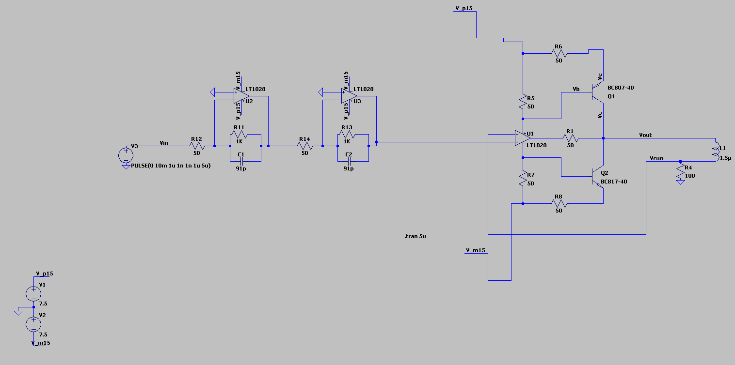
Hello , i have designed with a big help from this forum a driver.
at first glanse it amplified great the signal how ever when i probed R1 resistor as shown below on my lab scope with DC input , i saw oscilations.
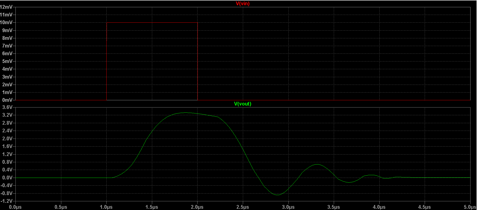
Now when i did step responce of the circuilt as shown below i see the oscilations.
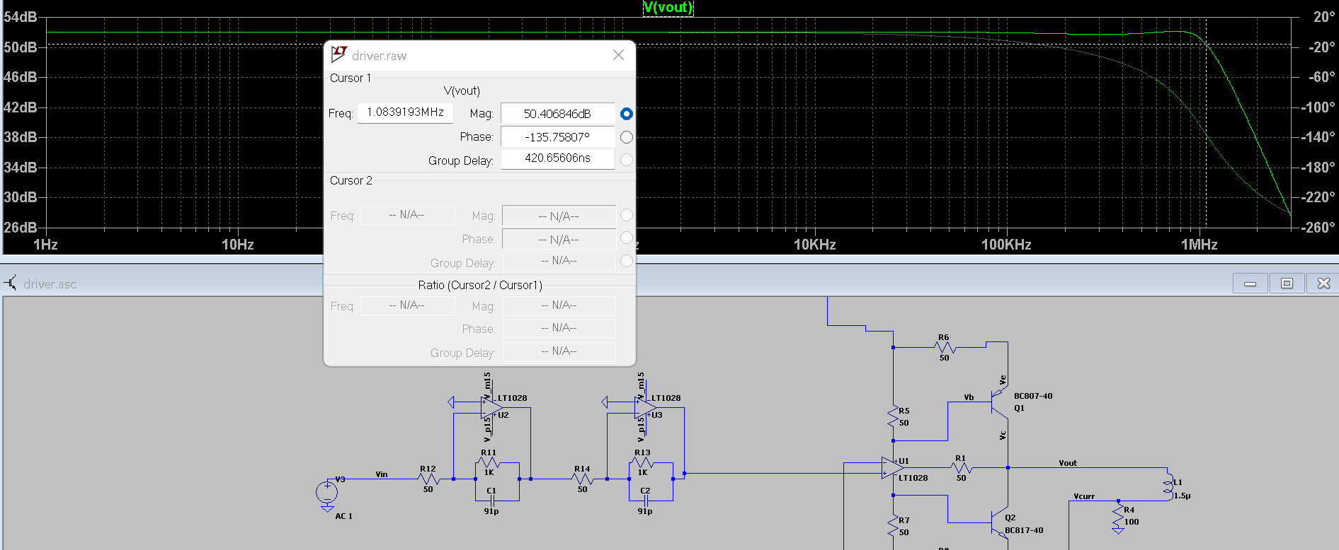
I also know from analog design course that i can try and see the AC responce.
LT1028 is -1 stable ,how does it influence the connection between the stages so i will not get oscilations.
What could cause instability in such configuration?
Thanks.

1704747020456.png


1704745962928.png

1704746912539.png


1704746711098.png
 
Hello Klaus, i just want to undestand how to deal with stability in real life.
suppose i have an unstable circuit.
I put DC as input however instead of getting DC output i get sine wave .
how can i link it to the barkausen condition of regular AC responce and see the phase margin situation?
Suppose i have AC responce as shown below, ( there is no situation where i have 0dB and 180 degress) so there is no barkausen condition?

1704921151178.png
 
Hello Dana, I know the theory i need to know based on what i see on the scope to understand where i stand with the phase margin situation.
Is there a method you can reccomend?
Thanks
 
Show a block diagram of your setup with cable type and lengths and where you choose common ground and how you measure current.

Also when you change one thing like coil current is screws up all the power balance design I had for 50 mA where they were all cool.

So are you happy with 20 mA +/-7.5V or will change?

Show exactly the schematic and testpoint for each waveform. Not old ones with +/-15V

if you supply a block diagram with your specs, I can help. Otherwise not.
--- Updated ---

You waves have a period of ~ 0.7us or 1.4 MHz which is the GBW value of the preamps. This why I had to add RC to the feedback of each stage due to the under-compensated LM1028. You do not have this so it gets amplified alot.

This IC is a poor choice for many reasons, but you insisted it could not be changed.
Your whole design/debug process needs an upgrade.

Start with complete specs to include and exclude certain behaviors with limits and characteristics of every sub-block in your system.
You haven't done this yet. Cable lengths and ground connections and supply noise matters. Measure & Specify it.
--- Updated ---

Hi,

the problem is that you ignore how an inductance works.

dI = V/L

it says: if you want a high rise rate in current (like the edge in a square wave) --> you need to apply a high voltage.

But for the advantage of low power dissipation you reduced the voltage. Now you miss the voltage to achieve a rectangular current waveform.

I can´t remember that you specified a rectangular waveform before. Maybe you did. If you did not: don´t complain!

Klaus
dI/dt = V/L doesn't convert to sine easily but essentially makes the load drop very little voltage compared the Isense resistor.
The problem is converting the pulse with gain of 50 in an under compensated OA with a boost in high Q gain and phase shift towards resonance.
This is all due to reducing pulse input voltage, supply voltage and lack of compensation given and basically not following directions.
 
Last edited:
There is no reason given why you only supply a 10 mVp pulse then distort it with 2 stages of underdamped gain.

When you could supply a 5V pulse with CMOS logic easily.
Then skip the 1st two stages.

This design follows no logical process without specs or reasons or purpose. or a block diagram with details!
--- Updated ---

Hello Klaus, i just want to undestand how to deal with stability in real life.
suppose i have an unstable circuit.
I put DC as input however instead of getting DC output i get sine wave .
how can i link it to the barkausen condition of regular AC responce and see the phase margin situation?
Suppose i have AC responce as shown below, ( there is no situation where i have 0dB and 180 degress) so there is no barkausen condition?

View attachment 187743
This is normal for this model, unfortunately there is no model to use the external compensation pin to simulate that. Another reason not to use this IC for this purpose.
That requires skill and breadboarding. Precompensation can yield 90 deg phase margin with loss of BW. and its spelled Barkhausen
 
Last edited:
For CMOS cable use STP wire or coax and add series R to match cable impedance. Zo=Vol/Io STP ~ 200 Ohms

@danadakk , the Phase/gain margin is complicated by an under-compensated O.A. here. These margins in higher order OA's tend to follow root locus or Nyquist plots more accurate but are fine for 1st order compensated gain/phase margins. i.e. They must be 1st order near the zero crossing for gain or phase to same predictions for ringing. But here, he just needs 20 mA step response, and over-complicated with over-heating, over voltage, current-amplify topology that is not a 1st order compensated Op Amp and with wide current process variables is not ideal for such a simple requirement. Yet he is unwilling to share more info. Must be top secret. :cool:
 
Last edited:
Pretty long discussion, a very basic information is still missing: required driver bandwidth. It's absolutely necessary to start compensation or possible redesign of the driver.
 
Hi,
Suppose i have AC responce as shown below, ( there is no situation where i have 0dB and 180 degress) so there is no barkausen condition?
often it´s the problem between simulation and real circuit.

A bad PCB layout may shift phase and gain.
Missing power supply capacitors in the real world.
Or even the scope probes may influence stability.
Even possible: you see some measurement artefact.

Indeed this is the reason why I don´t use simulations that often.
If you want to simulate an almost "realistic" circuit you need to input a lot more details. Like inductive coupling, stray inductance, stray capacitance .. of every node.
But as soon as you are aware of these "problems" you are 90% on the safe side, because you automatically improve the PCB layout to minimze these errors.

So a "simple" simulation sometimes is not very helpful.
A "detailed simulation" may be rather complicated to draw, time consuming and still not accurate enough.
So best would be to have a tool that uses the PCB layout informations automatically. But often these tools are expensive.

*****

My way:
* I´d say I´m rather experinced with optimizing PCB layouts.
* besides this ... I collect my circuit requirements (like frequency response) ... and go a simple but rather safe way by using local feedback to ensure stability.

This way - for stability - I exclude the whole path: OPAMP_output --> current booster --> coil (phase shift) --> shunt --> feedback to OPAMP. and the involved wiring.
So my "safety feedback" for stability often is just a capacitor from output to inverting input in combination with a R in the feedback path.
BUT: for this simplified solution you need a "unity gain stable OPAMP".

In your case:
* I´d limit the input frequency .. just to avoid that high frequency is being introduced (1)
* then I´d use a feedback using Rs and Cs (from OPAMP output to inverting input) for high frequencies.
It´s a question of the application´s requirements where to set the cut off frequencies .. both of the wanted current (I) feedback as well as the stabilizing capacitive feedback.
And of course it´s a question of the used OPAMP. Like in case of the LT1028 you can´t use a simple capacitive local feedback because this means a gain of +1 at high frequencies and in this case the OPAMP is not stable.

***
(1)
You´ve already use two OPAMPs with low pass filters. (Simply these filters don´t allow clean square waves. You need to be aware of this. )
But I often use a series R and a C to GND (close at the OPAMP input) to even suppress introduced noise. This passive way has improvements in not_introducing new noise (like OPAMPs do) and to suppress existing noise up to very high frequencies.

Klaus
 
FWIW his scope matches my simulation without his design.

Non-inverting amplifiers are more stable than inverting ones, but in this case not enough without matching crossover currents to zero crossing pulses stimulus.

A bandaid won't fix it very well.

AD8033 works pretty well. right? But probably banned for export to his location. But then Armenia can get it.
 
Last edited:
Hello ,The heart of the story is the inductor of the YIG.I understand that this PCB is problematic and i need to produce a new one.
I need to construct a device in which we input 1mV DC and we get of the coil output 20mA DC.
The LC meter shows L=6.04uH and Cx=0.015uF.
The input to the device is DC there is no need for bandwidth. (because YIG works purly on DC)
What OPAMP do you reccomend me to use, so it will be low noise and stable?
given my goals Could you please reccomend me some structure i can try and simulate with this opamp?
Thanks.

1705000371346.png
 
Non inverting seems much more stable.


1705014638537.png


Regards, Dana
 

Attachments

  • 1705014499783.png
    1705014499783.png
    207.1 KB · Views: 33
Hello ,The heart of the story is the inductor of the YIG.I understand that this PCB is problematic and i need to produce a new one.
I need to construct a device in which we input 1mV DC and we get of the coil output 20mA DC.
The LC meter shows L=6.04uH and Cx=0.015uF.
The input to the device is DC there is no need for bandwidth. (because YIG works purly on DC)
What OPAMP do you reccomend me to use, so it will be low noise and stable?
given my goals Could you please reccomend me some structure i can try and simulate with this opamp?
Thanks.

View attachment 187795
>" The input to the device is DC there is no need for bandwidth. (because YIG works purely on DC)"

wrong answer.

The current source controls the deviation of freq of the YIG and in order for the PLL to work it in a closed loop to capture the maximum error frequency out of the filtered phase mixer.

How much freq. error is worst case? This demands a high bandwidth. ( Much more than 10 kHz.)
So you may program a sweep if you have a "lock detector" . Then at what rate MHz/s. This also needs bandwidth.

Why are you unable to articulate design specs? You must try.

According to your RLC measurements the Self Resonant Freq. (SRF) is 500 kHz so the bandwidth (BW) must be far less.
1705016639030.png


All inductors have resistance at DC or DCR.
You measured
1mV DC and we get of the coil output 20mA DC
i.e. DCR = ~ 0.05 ohms.

The goal is not to measure 1 mV DC.

It is to get it to oscillate and at the right fo then control that frequency & phase error to 0. It helps to know I/O specs.
Like input RF and current levels vs output and distortion. Then derive the offset error and gain of A/Hz gain and DC current to null offset, all which are TBD...
.
The transfer function and nominal value have yet to be defined.

This current may have an insufficient magnetic field to operate properly and require improved magnetic pole pieces.
I expect maybe some time next year when the current amplifier gets defined. Even a common emitter current source BJT with a AAA battery would work better spurious free than his design.

The signal is amplified with a common base (CB) or CG FET with high impedance L on base or gate with matching network on output. It oscillates at a frequency proportional to an externally applied magnetic field when excited in a different direction by an RF field.

Non inverting seems much more stable.


View attachment 187801


Regards, Dana
Thanks for illustrating my previous point which was included in my bandaid Rev C here.

The previous comment about YIG non-linearity is not the current control but the hysteresis can be as much as 10 MHz ! Which is a lot more than the bandwidth of this current source. So I expect this is all a waste of time until the OP figures how this is supposed to work and what specs are needed before wasting more time.
 
Last edited:
Non inverting seems much more stable.
Thanks for the simulation. Very interesting.

In both cases the non inverting input is low impedance.
The impedance of IN- however differs in both cases.

Thus I wonder how the "ringing" is influenced by the feedback impedance.

Does the output waveform look similar if the non inverting circuit has 10k (or 5k) as feedback resistor?

Klaus
yes the TIA capacitance and load L with series Rs form a series RLC resonance where it is almost critically damped for the values I used. But when used with Resistive loads it is not affected except when at minimum closed loop gain. So Vin+ is always low BW but with more damping factor. This become when Vin+ is used both virtual null inputs are moving with the input, against the input Cin, while when the Vin- is used , Vin+ is fixed DC so there are no input ac currents to reduce BW. (I think )
 
Yes Miller/strays of input + Rfdbk would affect :

1705025716643.png


Its all about noise G, in case of NI G is always >= 1, whereas INV can be anything..


Regards, Dana.
 
Thanks for the simulation. Very interesting.

In both cases the non inverting input is low impedance.
The impedance of IN- however differs in both cases.

Thus I wonder how the "ringing" is influenced by the feedback impedance.

Does the output waveform look similar if the non inverting circuit has 10k (or 5k) as feedback resistor?

Klaus
yes although in both cases, the Miller or input capacitance and load L with output series Rs form a series RLC resonance where it is almost critically damped for the values I used. But when used with Resistive loads it is not affected except when at minimum closed loop gain. So Vin+ is always low BW but with more damping factor. This become when Vin+ is used both virtual null inputs are moving with the input, against the input Cin, while when the Vin- is used , Vin+ is fixed DC so there are no input ac currents to reduce BW. (I think ) In some cases of bias balance I could get away with Rs=0 but not always. Normally the IC was current limiting on one polarity or the other while the BJT's boosted the drive current since the OpAmp could not drive 20 mA or even 50 mA, like the one I chose.

My RLC chart show 20 Ohms would be near ideal with 10uH yet the RLC meter shows a lower inductance without any load capacitance in my simulation.

This stresses the importance of characterizing the specs for each component and cable and the obvious of having design specs before even starting to layout a board and choose an IC.

Yes Miller/strays of input + Rfdbk would affect :

View attachment 187807

Its all about noise G, in case of NI G is always >= 1, whereas INV can be anything..


Regards, Dana.
It's not internal or source noise but the lack of closed loop margin near crossover causing a resonance there from meeting the Barkhausen Criteria but poor for a step input response. The pulse input provides the spectrum stimulation. I found slightly better responses with a Rs sense load resistor on Vin- than @dana's simulation and that the driver impedances were different in each state causing less ringing on the rising pulse above 0V and more ringing returning to 0. When output Rs = 200 the falling signal became much over damped by comparison. But this is not useful for this to be used as this design needs to be tossed.
--- Updated ---

Did anyone find something to be improved here?
1705027166944.png
 
Last edited:
Hi,

Thanks Dana again for the simulation.

The datasheet says LT1028 is stable with inverting circuit and A = -1.
So your inverting setups show ringing. Quite expectable.

But I was surprised by your first non inverting setup showing very stable condition on A = +1, while the datasheet says it is not stable.

Now the second setup with feedback resistor meets more my expectations. Lots of ringing, at the edge to oscillate.

Thanks again.

On the other hand the LT1028 is a very low noise OPAMP. It has an input noise less than a 50 Ohms resistor. So noise wise it makes no sense to use input impedances higher than those 50 Ohms.
An often with that low noise ... one needs an amplifier with high gain. So with high gain and low input impedance the LT1028 works great. I uset it this way in some high end audio circuits decades ago.

*******

So the conclusion to this thread is, that the LT1028 is not the best choice for this application. The application does not need that extremely low noise but it needs stability. I still vote for local feedback combined with the use of a unity gain stable OPAMP. But indeed I still don´t understand what the OP really wants to achive. The requirements regarding timing, the freqency range ... the true goals.

Klaus
--- Updated ---

Its all about noise G, in case of NI G is always >= 1, whereas INV can be anything..
Absolutely.
In your simulation inverting circuit, A=-1 , the noise G is +2.
Noise G is always >= +1 if I´m not mistaken, independent of external circuitry (inverting, non inverting, sum, integrator, differentiator...). (never below 1, never negative)

So without feedack resistor we have (noise G wise)
* low impedance
* high bandwidth

Adding a feedback resistor increases the gain ... and according datasheet: higher gain means better stability.
Datasheet says it is not stable at G=+1, but it is stable at G of +2 and higher. We see the opposite.
Thus - imho - the problem we see in the simulation is not simply the gain, but the phase shift introduced by the feedback resistor in combination with capacitance of the input pins.

Klaus
 
Last edited:

LaTeX Commands Quick-Menu:

Similar threads

Part and Inventory Search

Welcome to EDABoard.com

Sponsor

Back
Top