anhnha
Full Member level 6
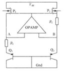
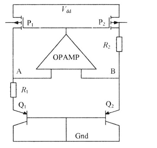
I am measuring phase margin for this bandgap using iprobe from analogLib in Cadence by breaking the loop and inserting iprobe between the output of op amp and gate of two top transistors. However, the problem is that I have heard that this method doesn't work for circuit that has more than one loop.
If so, how can I measure phase margin in Cadence for this type of bandgap?
Any help is appreciated!
If so, how can I measure phase margin in Cadence for this type of bandgap?
Any help is appreciated!