soroosh1234
Newbie
Hi,
I'm trying to create a transformer on SiGe .13um. When I add 4 ports that are referenced to the ideal ground in momentum everything is fine and I'm gettign my desired performance.
But when I add the ground plane which the grounds of the G-S-G pads are connected, I lose my performance and it seems the return current path to the ground has some inductance. The distance of the ground plane with my outer turn is is around the radius of my transformer.
I wanted to know how should I define the ports to correctly account for the ground ports of GSG probe.
And also what are the design guideline of a transformer.
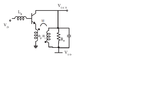
One terminal of the primary is connected to VCC and one terminal of secondary is connected to ground.
Your help is really appreciated.
I'm trying to create a transformer on SiGe .13um. When I add 4 ports that are referenced to the ideal ground in momentum everything is fine and I'm gettign my desired performance.
But when I add the ground plane which the grounds of the G-S-G pads are connected, I lose my performance and it seems the return current path to the ground has some inductance. The distance of the ground plane with my outer turn is is around the radius of my transformer.
I wanted to know how should I define the ports to correctly account for the ground ports of GSG probe.
And also what are the design guideline of a transformer.
One terminal of the primary is connected to VCC and one terminal of secondary is connected to ground.
Your help is really appreciated.