Continue to Site

Welcome to EDAboard.com

Welcome to our site! EDAboard.com is an international Electronics Discussion Forum focused on EDA software, circuits, schematics, books, theory, papers, asic, pld, 8051, DSP, Network, RF, Analog Design, PCB, Service Manuals... and a whole lot more! To participate you need to register. Registration is free. Click here to register now.

offset control circuit

Status
Not open for further replies.

franticEB

Full Member level 3
Full Member level 3
Joined
May 10, 2010
Messages
153
Helped
1
Reputation
2
Reaction score
2
Trophy points
1,298
Visit site
Activity points
2,551
Hi, i've found the circuit shown in figure below
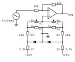
ib6fin.jpg

the circuit connected to the positive pin of operational amplifier seems to be useful to regulate the offset of OP AMP by trimming the value of resistors R1 and R2.

I don't understand how this circuit works and how it is able to regulate the offset, could you help me please?
 

All opamps need to be "balanced" as they are typically powered from +/- 15 VDC power supply, center is ground. For a "fine tuning" the circuit shown can be used, with the two 5k potentiometers you can adjust output voltage exactly to zero for a zero input (inveting opamp input). The diodes shown can be Zeners for regulation.
Some opamps have a pair of pins (1 and 8) to which to connect a potentiometer with the slider to +15V for the same balancing.
 

the diodes are not zener...

But i've not understood yet how this circuit works...
 

the diodes are not zener...

But i've not understood yet how this circuit works...

Do you know what an offset is? If so, then you can reduce it by the fine balancing, and the circuit shown is designed for that. You can use a potentiometer connected between + and - 15V but i is too coarse. Here you have two voltage dividers, so the 5k trimmers adjust the offset compensation by millivolts.
 

Hi, i've found the circuit shown in figure below

View attachment 97044

the circuit connected to the positive pin of operational amplifier seems to be useful to regulate the offset of OP AMP by trimming the value of resistors R1 and R2.

I don't understand how this circuit works and how it is able to regulate the offset, could you help me please?

Lets start with the diodes. These are connected forward conduction with 3.3k in series. A typical diode would have a drop of around 0.7v (silicon). So the pin of diode which is away from gnd would be at ~ +0.7v and -0.7v.

Now the 10k and 1K setup. This further divides the 0.7v down to 0.7 * 1/11 = 0.064 V (approx, not considering the 5k trimpots for the moment).

So now we have two potentials which are ~ +0.064 and -0.064 around gnd.

The 5k trimpots are connected across this, and their junction voltage can hence be varied between these values, which is fed to the + of the opamp.
With a gain of ( 1 + 40K/10k) = 5, this small voltage at the + input will result in the output being "offset" in a range of ~600mV ( 0.064 x 5 x 2)

Does that make sense ?

p.s. those trimpots aren't an elegant method. Who designed this topology ?
 
It is an old design....
how would you suggest to improve the design?

franticEB, just to avoid misunderstandings or too much work (on your side):

Of course, we can discuss here several other schemes to compensate offset voltages.
However, you should know that in most cases such an offset compensation is NOT necessary. It really depends on the particular application.
So - what is your task? To study offset compensation methods or to use an opamp for a special purpose?
 

With a gain of ( 1 + 40K/10k) = 5, this small voltage at the + input will result in the output being "offset" in a range of ~600mV ( 0.064 x 5 x 2)

just to be precise the gain is 40K/10k, because the configuration is inverting
 

just to be precise the gain is 40K/10k, because the configuration is inverting

Just to be precise: The relevant gain is (1+40/10)=5.
Noise always is amplified with the "noise gain" which is identical to the non-inverting gain - independent on the sign of the signal gain.
 

Just to be precise: The relevant gain is (1+40/10)=5.
Noise always is amplified with the "noise gain" which is identical to the non-inverting gain - independent on the sign of the signal gain.

Hi here is inverting amplifier the gain is -Rf / Rin = - 40 / 10 = - 4;

you can use the 1st and 5th pins of 741 op amp to directly control the offset..for different op amp for connections to control the offset refer the corresponding op amp data sheet......
 

Hi here is inverting amplifier the gain is -Rf / Rin = - 40 / 10 = - 4;
you can use the 1st and 5th pins of 741 op amp to directly control the offset..for different op amp for connections to control the offset refer the corresponding op amp data sheet......

I repeat: An inverting amplifier with a gain of "-4" amplifies all internal voltages (noise, offset) with the so called "noise gain" which is in this case (1+4)=5 !
 

Just to be precise: The relevant gain is (1+40/10)=5.
Noise always is amplified with the "noise gain" which is identical to the non-inverting gain - independent on the sign of the signal gain.

ok I apologize for the inaccuracy, did not mean to be rude... ;-)

so for the analysis have i to focus my attention on noise gain?
Could you explain me better this point? is it the noise figure?
 

I repeat: An inverting amplifier with a gain of "-4" amplifies all internal voltages (noise, offset) with the so called "noise gain" which is in this case (1+4)=5 !

How do you saying it was +1 why its not +2 ??
for Rin = 1k , Rf = 1k with input of 1 V what will be the output voltage ??
 

How do you saying it was +1 why its not +2 ??
for Rin = 1k , Rf = 1k with input of 1 V what will be the output voltage ??

* The non-inv. gain formula is (1+Rf/Rin) and not (2+Rf/Rin).
* Your example: signal gain=-1 and noise gain=+2 (applies to noise and offset).
 

To refocus on the original discussion about offset, you can buy modern op amps with very low offset, such that you often don't need to add an offset correction circuit. And that offset is generally independent of the power supply voltages or the balance between supplies.
 

* The non-inv. gain formula is (1+Rf/Rin) and not (2+Rf/Rin).
* Your example: signal gain=-1 and noise gain=+2 (applies to noise and offset).

What are you talking about here we having inverting amplifier.. I asked about you put 4+1 and we are talking about it and I asked about how do you saying it was +1 and not +2 Is that clear??
 

What are you talking about here we having inverting amplifier.. I asked about you put 4+1 and we are talking about it and I asked about how do you saying it was +1 and not +2 Is that clear??

I am talking about the noise gain. It seems you don`t understand. Before asking "is that clear ?" it would be better for you to improve your knowledge and consult any textbook.
My recommendation: Make up your mind and try to find out that a signal that is applied at the left node of the input resistor (inverting amplifier) will NOT be amplified with the same amplification factor as an unwanted voltage that exists DIRECTLY between the input terminals of the opamp (like offset and noise voltages).
 

If you add a small voltage or noise source model directly in series with one of the op amp inputs and calculate the closed loop gain from those sources, you will see that it is amplified by the non-inverting gain, even if the op amp is being used in an inverting mode.

Similarly the closed loop gain bandwidth from the GBWP (Gain BandWidth Product) of the op amp is determined by the non-inverting gain, not the inverting gain of the circuit.
 

Status
Not open for further replies.

Part and Inventory Search

Welcome to EDABoard.com

Sponsor

Back
Top