mohamis288
Full Member level 3
I have recently created a project in ADS. It contains a couple of transmission lines, capacitors, and resistors. When I connect my transmission lines to the s2p file, transient simulation is done successfully. But, when I connect the large-signal model to transmission lines, a time step error is shown after about 120 ps. My component is an RF IC produced by NXP company. simulation models can be downloaded from the following link:
https://www.nxp.com/products/radio-...ed-amplifiers:AFIC10275N?fpsp=1#documentation
the large-signal model does not have any incompatibility with transient simulation, because I have done the simulation simulation on this ( without any other component, wire , transmission line and etc). My RF fundamental frequency is 1090 MHz. Also, I did s-parameter simulation on it successfully.
In order to solve the timestep error, I have taken the following measures:
-I have placed a 1e-6 pF capacitor at every node
-I have connected DC voltage supply to the IC with an intermediary 10 ohm resistor
-I have changed the "time step" parameter over a wide range from 0.01 ps to 100 ps
-I have enabled (or disabled) the "limit time step for transmission line" checkbox
-I have used different convolution tolerances (specially "strict" mode) and time step control methods
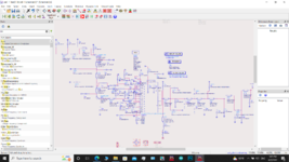
Here is the schematic:
.png")
I tried to upload my code, but its size was too much (even higher than 1 Gb).
The error message is represented in the following:
I have been thinking of solving this error for more than 2 weeks ,but I can not know how to solve this. It would be great if you can give me a couple of suggestions.
I have asked a similar question on the EDAboard, but here I asked it again with more clear details.
https://www.nxp.com/products/radio-...ed-amplifiers:AFIC10275N?fpsp=1#documentation
the large-signal model does not have any incompatibility with transient simulation, because I have done the simulation simulation on this ( without any other component, wire , transmission line and etc). My RF fundamental frequency is 1090 MHz. Also, I did s-parameter simulation on it successfully.
In order to solve the timestep error, I have taken the following measures:
-I have placed a 1e-6 pF capacitor at every node
-I have connected DC voltage supply to the IC with an intermediary 10 ohm resistor
-I have changed the "time step" parameter over a wide range from 0.01 ps to 100 ps
-I have enabled (or disabled) the "limit time step for transmission line" checkbox
-I have used different convolution tolerances (specially "strict" mode) and time step control methods
Here is the schematic:
I tried to upload my code, but its size was too much (even higher than 1 Gb).
The error message is represented in the following:
Code:
    Simulation Messages

Warning detected by hpeesofsim during netlist flattening.
    Inductor `FET2FSL1.X1.L1' L=-9e-11 is negative.
Warning detected by hpeesofsim during netlist flattening.
    Inductor `FET2FSL1.X2.L1' L=-9e-11 is negative.
Warning detected by hpeesofsim during netlist flattening.
    Inductor `FET2FSL1.X3.L1' L=-4e-11 is negative.
Warning detected by hpeesofsim during netlist flattening.
    Inductor `FET2FSL1.X3.L2' L=-4e-11 is negative.
Warning detected by hpeesofsim during netlist flattening.
    Inductor `FET2FSL1.X4.L1' L=-4e-11 is negative.
Warning detected by hpeesofsim during netlist flattening.
    Inductor `FET2FSL1.X4.L2' L=-4e-11 is negative.
Warning detected by hpeesofsim during circuit set up.
    Mutual inductor `FET2FSL1.X4.Q2.Mutual1' has an unphysical mutual inductance M=-7.061e-13.
    L1=0.000e+00 L2=0.000e+00; limit for M is +/-0.000e+00.
Warning detected by hpeesofsim during circuit set up.
    Mutual inductor `FET2FSL1.X4.Q1.Mutual1' has an unphysical mutual inductance M=-7.061e-13.
    L1=0.000e+00 L2=0.000e+00; limit for M is +/-0.000e+00.
Warning detected by hpeesofsim during circuit set up.
    Mutual inductor `FET2FSL1.X3.Q2.Mutual1' has an unphysical mutual inductance M=-7.061e-13.
    L1=0.000e+00 L2=0.000e+00; limit for M is +/-0.000e+00.
Warning detected by hpeesofsim during circuit set up.
    Mutual inductor `FET2FSL1.X3.Q1.Mutual1' has an unphysical mutual inductance M=-7.061e-13.
    L1=0.000e+00 L2=0.000e+00; limit for M is +/-0.000e+00.
Warning detected by hpeesofsim in topology check during circuit set up.
    Number of nodes with only one device attached (topology corrected): 1
Warning detected by hpeesofsim during TRAN analysis `Tran2'.
    Component `FET2FSL1.X4.SNP1.CMP1':
       ImpMaxFreq is reduced to highest data frequency at 8.000000e+09 Hz.
Warning detected by hpeesofsim during TRAN analysis `Tran2'.
    COMPONENT `FET2FSL1.X4.SNP1.CMP1':
       Highest frequency in data is 8e+09 Hz, which is smaller than the maximum source bandwidth 8.72e+09 Hz.
Warning detected by hpeesofsim during TRAN analysis `Tran2'.
    Component `FET2FSL1.X3.SNP1.CMP1':
       ImpMaxFreq is reduced to highest data frequency at 8.000000e+09 Hz.
Warning detected by hpeesofsim during TRAN analysis `Tran2'.
    COMPONENT `FET2FSL1.X3.SNP1.CMP1':
       Highest frequency in data is 8e+09 Hz, which is smaller than the maximum source bandwidth 8.72e+09 Hz.
Warning detected by hpeesofsim during TRAN analysis `Tran2'.
    Component `FET2FSL1.SNP3.CMP1':
       ImpMaxFreq is reduced to highest data frequency at 8.000000e+09 Hz.
Warning detected by hpeesofsim during TRAN analysis `Tran2'.
    COMPONENT `FET2FSL1.SNP3.CMP1':
       Highest frequency in data is 8e+09 Hz, which is smaller than the maximum source bandwidth 8.72e+09 Hz.
Warning detected by hpeesofsim during TRAN analysis `Tran2'.
    Component `FET2FSL1.X2.SNP1.CMP1':
       ImpMaxFreq is reduced to highest data frequency at 8.000000e+09 Hz.
Warning detected by hpeesofsim during TRAN analysis `Tran2'.
    COMPONENT `FET2FSL1.X2.SNP1.CMP1':
       Highest frequency in data is 8e+09 Hz, which is smaller than the maximum source bandwidth 8.72e+09 Hz.
Warning detected by hpeesofsim during TRAN analysis `Tran2'.
    Component `FET2FSL1.SNP2.CMP1':
       ImpMaxFreq is reduced to highest data frequency at 8.000000e+09 Hz.
Error detected by hpeesofsim during TRAN analysis `Tran2'.
    Internal timestep 9.58155e-16 too small at time 1.44486e-10.
I have been thinking of solving this error for more than 2 weeks ,but I can not know how to solve this. It would be great if you can give me a couple of suggestions.
I have asked a similar question on the EDAboard, but here I asked it again with more clear details.