Continue to Site

Welcome to EDAboard.com

Welcome to our site! EDAboard.com is an international Electronics Discussion Forum focused on EDA software, circuits, schematics, books, theory, papers, asic, pld, 8051, DSP, Network, RF, Analog Design, PCB, Service Manuals... and a whole lot more! To participate you need to register. Registration is free. Click here to register now.

[PIC] Not sure about PIC24FJ64GA002 PPS documentation

Status
Not open for further replies.

Alloy

Advanced Member level 4
Joined
Apr 3, 2016
Messages
116
Helped
0
Reputation
0
Reaction score
0
Trophy points
16
Activity points
1,003
Hey
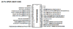
I have question about PIC24FJ64GA002 datasheet.

I think I know how OUTPUT remapping works:
The control schema of the Peripheral Pin Select is
extremely flexible. Other than systematic blocks that
prevent signal contention, caused by two physical pins
being configured as the same functional input or two
functional outputs configured as the same pin, there
are no hardware enforced lockouts. The flexibility
extends to the point of allowing a single input to drive
multiple peripherals or a single functional output to
drive multiple output pins.

So I can assign any function to output pins like RPn,
Value assigned to the RPn<4:0> pins corresponds
to the peripheral output function
number
and it's clear. Is that right?

But... what about INPUT pin?
For example, to which input pins I can remap the U1RX (UART1 Receive)??

There is a table in datasheet called "TABLE 4-30: PERIPHERAL PIN SELECT INPUT REGISTER MAP FOR PIC24EPXXXGP20X DEVICES ONLY" but I don't get how I should read it??
Can I map U1RX to any input PPS pin??
 

I believe the PPS documentation is rather clear.

Anyway, if you think about the purpose of PPS quite a bit, you'll realize that the assignment of input and output resources must be different.

Output functions are assigned to pins by a writing a function number to the output pin mapping register
Input pins are assigned functions by writing a pin number to the input function register.

This way you can assign multiple output pins to a single output function and multiple input functions to a single pin.
 
  • Like
Reactions: Alloy

    Alloy

    Points: 2
    Helpful Answer Positive Rating
Output functions are assigned to pins by a writing a function number to the output pin mapping register
This is clear, I have found:
"U1TX 3 UART1 Transmitit"
So I do (pseudocode, I will launch compiler later):
RP10R = 3; // output function number
And I understand that....

Input pins are assigned functions by writing a pin number to the input function register.
So I want U1RX...
"UART1 Receive U1RX RPINR18 U1RXR<4:0>"
I don't know what is what...
Register is RPINR18.
Configuration bits is U1RXR<4:0>.
"The RPINRx registers are used to
configure peripheral input mapping (see Register 10-1
through Register 10-14). "

Let's say I want to have U1RX on pin 11, how do I do that?
Simply RPINR18 = 11; ??
 

this is an example for a PIC24FJ64GB004
Code:
    RPOR2bits.RP5R = 0x0005;   //RA0->UART2:U2TX;
    RPINR19bits.U2RXR = 0x0006;   //RA1->UART2:U2RX;
 

So I've tried it in mikroC....


Code:
    // output - RP10 - U1TX
    RPOR5bits.RP10R = 3;
    // input - RP11 - U1RX
  //////////////  RPINR11bits.???? = ???;

/////////////////It seems that I can't map U1RX to RP11...

update:
Code:
    // output - RP10 - U1TX
    RPOR5bits.RP10R = 3;
    // input - RP11 - U1RX
    RPINR18bits.U1RXR = 11;
UART1 on RP10 and RP11 - is this correct now?
 

Attachments

  • PIC24FJ64GA002_pinout.png
    PIC24FJ64GA002_pinout.png
    59 KB · Views: 109

Status
Not open for further replies.

Similar threads

Part and Inventory Search

Welcome to EDABoard.com

Sponsor

Back
Top