Continue to Site

Welcome to EDAboard.com

Welcome to our site! EDAboard.com is an international Electronics Discussion Forum focused on EDA software, circuits, schematics, books, theory, papers, asic, pld, 8051, DSP, Network, RF, Analog Design, PCB, Service Manuals... and a whole lot more! To participate you need to register. Registration is free. Click here to register now.

Non PCB Mosfet Mounting

Status
Not open for further replies.

meltbox360

Newbie level 5
Joined
Dec 31, 2012
Messages
10
Helped
0
Reputation
0
Reaction score
0
Trophy points
1,281
Activity points
1,373
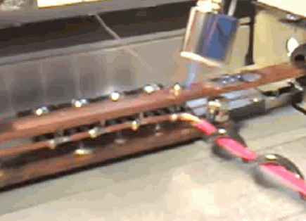
I can't seem to find anything on the topic of mounting high power Mosfets directly to hunks of metal to carry a bunch of current. How is such a thing done and does anyone have a link to someplace I could look at to get a good idea of the property way to connect the drain, sink, and gate if I wanted to use metal bars to carry power. Thanks.

Edit: I found this but it's just tons of solder on a PCB and seems difficult to do properly.https://ecomodder.com/forum/showthr...ion-programable-100amp-200amp-100v-13865.html

I have also come across a YouTube video showing a 200 amp motor controller but I can deduce exactly how the Mosfets are mounted.
 
Last edited:

the main connections are for the drain and the source pins which carry the high current. the wires need to be as thick and as short as possible and also be made of material which has the best conductivity -- so that overall the resistance is as low as possible.

if you are carrying 200 amps, then even a 10milliohm resistance will drop 2 volts ! And have to dissipate 100watts !!

so connecting many mosfets in parallel helps reduce the current each one must carry. the metal bars are not meant to actually carry this current - i think they are heatsinks to dissipate the mosfets power. depending on whether the drain or the source is connected to the body of the mosfet, and how they are connected in the circuit, then this heatsink can also be used to carry some current without use of insulating washers.
 
But how about the YouTube video showing a 200 amp device. It looks like the Mosfet is conducting through solid copper bars. I would prefer such a solution if possible.
 

But how about the YouTube video showing a 200 amp device. It looks like the Mosfet is conducting through solid copper bars. I would prefer such a solution if possible.

can you post the url so that we can also see and comment ?
 
For very high power applications, semiconductors will come in "modules," which are usually meant to mount to a heatsink via an isolated heat spreader, and have screw terminals for the high power connections. Do a google image search for "IGBT module" and look at the results, you'll get the idea.

Normally the terminals will connect to some heavy bus bar, or heavy gauge wire with ring terminals. Lower power signals (like gate drive) usually have separate connections on the module which can be pins, spade lugs, or smaller screw terminals.
 
Modules do seem rather expensive though. Is there no good way to do it without them?
Look sharp! Quite obviously, there are no MOSFET modules shown in the youtube video. It's just a number of standard TO-247 packaged devices soldered to copper bus bars. There are other videos from the same author that show more clearly how it's made.
 
Concerning power mosfets encapsulated in pack case, assemblable w/ screw, can be interconnectable w/ stack metalic plates, properly isolated.

It makes easier build the power stage, and also restrict current flow into a confined region.

I saw this concept with a pack IGBT set on a 5KW UPS based on Push-pull topology, allowing a very clean design.


+++
 
Modules do seem rather expensive though. Is there no good way to do it without them? For a hobby project. Definitely not production.
This is the part where you start looking at industrial surplus stores for old motor drives and power supplies, buy them for pennies on the dollar and salvage the perfectly functional power components inside. I've been able to pick up thousands of dollars in semiconductor modules this way, practically for free.
 
Thanks for the surplus suggestion. To be honest I watched each video I could find from the 200 amp youtube videos and it was way to blurry to see much of anything except that there is a ton of copper where the three pins of the mosfets are. Is it safe to for example bend the pins of a mosfet and still expect it to function to spec? Then I can see how things could be connected.
 

Concerning sugestion I had presented on post #8, find bellow a draft explaining the concept :

PLATE.JPG

Observe that interconnections are performed by module screw, and other points are avoided due to other larger holes.

+++
 
To be honest I watched each video I could find from the 200 amp youtube videos and it was way to blurry to see much of anything except that there is a ton of copper where the three pins of the mosfets are. Is it safe to for example bend the pins of a mosfet and still expect it to function to spec? Then I can see how things could be connected.

I was referring to the video that shows how the drain bus is soldered. It's clear enough to be read as an instruction I suppose. I see that with about no clue about handling of electronical components (e.g. if transistor pins can be safely bent) additional information might be needed.

1586443700_1357384652.gif


As a middle course between "non-PCB" mount of transistor with regular packages and expensive modules, screw connected SOT227B package might be considered.
 

Find bellow a few more detailed draw, now explaining final assembly, and connection entries :

PLATE_5.JPG

+++
 
Last edited:

Status
Not open for further replies.

Part and Inventory Search

Welcome to EDABoard.com

Sponsor

Back
Top