Continue to Site

Welcome to EDAboard.com

Welcome to our site! EDAboard.com is an international Electronics Discussion Forum focused on EDA software, circuits, schematics, books, theory, papers, asic, pld, 8051, DSP, Network, RF, Analog Design, PCB, Service Manuals... and a whole lot more! To participate you need to register. Registration is free. Click here to register now.

New bee wants to know that the mistakes in the circuit

Status
Not open for further replies.

MADSOH

Newbie level 4
Joined
Jan 29, 2013
Messages
5
Helped
0
Reputation
0
Reaction score
0
Trophy points
1,281
Activity points
1,313
New bee wants to know about the mistakes in the circuit

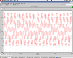
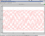
In the images below we have given the circuit that we have designed in cadence what are the changes we can make to get an improved output??????? and this circuit is designed for strong inversion what are the changes that we can make so that it works in weak inversion?????? screenshot1 is our circuit, screenshot 2 is our input, screenshot 3 is output from the source of M15 and screenshot 4 is output from the source of M7
 

Attachments

  • Screenshot-1.png
    Screenshot-1.png
    79.9 KB · Views: 88
  • Screenshot-2.png
    Screenshot-2.png
    67.6 KB · Views: 69
  • Screenshot-3.png
    Screenshot-3.png
    60.8 KB · Views: 74
  • Screenshot-4.png
    Screenshot-4.png
    66.6 KB · Views: 72
Last edited:

what do you mean by improved output? if you mean increased gain, why not incerase resistance of load transistors or using wider input transistors! your input transistors are very smal (not wide), why? and is there a reason for the reason for the different output DC voltage or not? check these. also, why do you want it to operate in weak inv? Is it only lower power cons? if so, and you have considered the resulting lower bandwidth, higher missmatch and ...., then for example for the input stage you can do so by lowering the tail current i.e. lower gate voltage for M5 (make sure that this transistor has a high enough VDS to be in saturation) , meaning higher source voltage for M0 and M3. Also, are you using a tripple well process? if not, dont connect the bulks fo the NMOS devices to their sources. Connect bulks of all nmoses to ground.
 

Status
Not open for further replies.

Part and Inventory Search

Welcome to EDABoard.com

Sponsor

Back
Top