Continue to Site

Welcome to EDAboard.com

Welcome to our site! EDAboard.com is an international Electronics Discussion Forum focused on EDA software, circuits, schematics, books, theory, papers, asic, pld, 8051, DSP, Network, RF, Analog Design, PCB, Service Manuals... and a whole lot more! To participate you need to register. Registration is free. Click here to register now.

need help with my first pll transmiter rdvv300 won't lock stay busy please

Status
Not open for further replies.

Dreamingworld

Newbie level 4
Newbie level 4
Joined
Feb 6, 2014
Messages
6
Helped
0
Reputation
0
Reaction score
0
Trophy points
1
Visit site
Activity points
60
hi,

I recently made my first FM pll transmitter Rdvv 300mW found here: http://www.3-mtr.info/shareware/RDVV 300mWatt

The pic, the buttons, the lcd are working but the TSA5511 chip cannot lock, the led are not activate and on the lcd stay on "busy"

i have double check the board before solder for short circuit and its ok, and double check my solder before power on ,when i put the power on without all chip i check if all voltage are good and they are ,chek the the polarity of the transistors and it's good

i don't have any experience in colpits oscillator, i don't know how that work and if it oscillate, but i have study the tsa5511 and i know how she work and how to program it (i use a genium phillips chip)

I have a 20 MHz oscilloscope Hantek 60200be

http://www.hantek.com/en/ProductDetail_2_31.html

a multimeter as any technician

and a frequency counter victor 3165 (VC3165)

**broken link removed**

to help me in my debugging

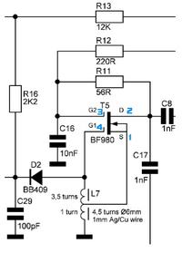
and the partial shematic i found on internet

schemardvv3000001.jpg


please help me to debug it i have already spent a lot of time to understand but i am on the same point :the transmitter doesn't work

thanks
 

"...and the partial schematic i found on internet..."
So, you started to build a circuit without having the full schematic?

T5 (BF980 dual-gate MOSFET) is the oscillator. This is ECO type oscillator (Electron Coupled Oscillator) using a tap on the inductor. If the tap is not in the right place, the oscillator cannot get enough feedback to oscillate.
Your frequency counter VC3165 (up to 2.4GHz and 30mV sensitivity) should be fine to see if the oscillator works, which probably oscillate around 100MHz.
Try to measure the oscillation using the frequency counter at pin RFIN1 of TSA5511.
If the oscillation is there, check the serial programming (SDA SCL) of the PLL chip, because if this is not correctly done the PLL will never lock.
Also if the PLL is not locked you don't get TX output enable at P2 of the PLL chip. This prevents to transmit if the PLL is not locked.

Hi,

thank you for taking time to help me.

regarding the scheme, what I mean is that any partial order part is missing on this one, but the whole party and oscillator amplifier is complet.Je board not found another diagram of the rdvv300 full internet and the link provides the issuer does not propose scheme, it does not discourage me to launch into the adventure, but I was far from me imagined that ask as many problems.

I'll try to find out if there is a measurable frequency on pin 15 (rfin1) of tsa5511 and will keep you informed

in the communicaton concernet i2c it seems to be because when I OPERATIONAL apppuis on the button set the red LED lights up and I can change the frequency, I check to the oscilloscope and I saw the answer to tsa5511 microcontroler the only thing I find strange is the frequency of the clock but for me it communicates

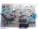
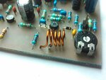
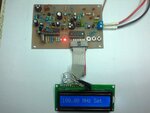
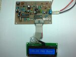
Here are pictures of my achievement

IMG_20140206_145436.jpgIMG_20140206_145514.jpgIMG_20140206_145817.jpgIMG_20140206_145840.jpgIMG_20140206_150035.jpg


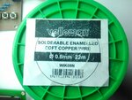
i make the coil as describe

L1 = 4.5 turns, 6 mm internal diameter, 0,8 mm in place of 1 mm (CuAg????), tap ¾ to 1 turn from ground (spaced)

with that

https://www.velleman.eu/products/view/?country=fr&lang=fr&id=376218

if there are something wrong please let me know

thanks
 
Last edited:

hi,

i have just check if there is a on ascillation on RFIN1 of the tsa5511 and i can't get it on my victor 3165 frequency conter

maybe the eco not oscillate but i don't know why!!

i use bf981 mosfet transistor and bb809 varicap
maybe the polarity is wrong but i don't know how to chek it
I relied a long pin for connection symbolized by a thick line in the diagram layout and technical documention component

can anyone can say me why and help me please i have also make a new coil chek connection without result

please
 

Replace BB809 with a 33pF capacitor to be sure the varicap is not the cause, and also tap the oscillator inductor (L7) in the middle. This will give the maximum feedback for an ECO type oscillator. With the values given you should have about 1V amplitude of a signal around 100MHz.
 

I would break the PLL DC loop, because I would think in the "busy" mode this is being swept to try to get a lock. So cut the PCB track between C23 and C21, this is to leave R13 and R16 putting the maximum reverse bias on the Varicap. Like this the oscillator should be higher in frequency then its normal range. Then try to get the oscillator to go at F +20% or so.
Frank
 

HI ,

I think I found why the oscillator does not work and if I'm right I'm an idiot for not having thought .

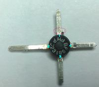
As I said this is my first fm transmitter and in addition I chose a pll version, so this is a big first for me in the use and welding mosfet has 4 pins, thereby for the implementaion of it on the map I have focused on the longer pin ( pin 2) telling me that if it was then it puts others as default , because if I was wrong we return the following horizontal pin 2 and 4 remain in their place , but they pin 1 and 3 are reversed.

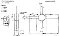
which leads me to know where is the pin 1 and datasheet gave me the solution, a small tab located at the base of the pin and this one while not on other pins , and if the scheme with bf980 remains valid with the implementation of bf981 I use, so I wired in reverse

before I get into the modifation to test you offer me I would like to have confirmation that it is welded upside down , eventuelement know if it could be blown around and what other component suffered before continuing

in Figure 1 as it is connected to my board
in Figure 2 as I think it will have to be


please , thanks
 

hi,

I have corrected my mistake and put the transistor in its correct polarity and now tsa5511 locks the frequency and the transmitter works (must be taken to be learned).

after my test, it turns out that it does not lock above 98 MHz with frequency of my conpteur I see it oscillate around 99 Mhz without ever locked


how can I make it locks the entire FM band?

please
 

Maybe at higher frequencies the level of the oscillator is dropping bellow the limit of RFIN1 (< 300mV - you cannot see this with your frequency counter which has 30mV sensitivity) .
And second, it is possible the varicap to don't get enough voltage for high frequency range, and the oscillator is losing the lock control.
 

Status
Not open for further replies.

Part and Inventory Search

Welcome to EDABoard.com

Sponsor

Back
Top