Continue to Site

Welcome to EDAboard.com

Welcome to our site! EDAboard.com is an international Electronics Discussion Forum focused on EDA software, circuits, schematics, books, theory, papers, asic, pld, 8051, DSP, Network, RF, Analog Design, PCB, Service Manuals... and a whole lot more! To participate you need to register. Registration is free. Click here to register now.

[SOLVED] Need help to analyse a power supply circuit! (LM317 / LM337)

Status
Not open for further replies.

Gauthier

Newbie level 6
Joined
Nov 2, 2011
Messages
13
Helped
2
Reputation
4
Reaction score
2
Trophy points
1,283
Activity points
1,404
BA Double corriger corriger.JPG

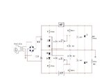
At school I had to build this circuit on a protobaord, I started from the left to the right testing it between each layer. Everything was fine until I plugeg the 10uF capacitor on the negative side of the power supply.

Both 10uF capacitors are there to filter the noize that the potentiometers might be producing...

On the positive side, the 10uF capacitor have no effect or minimal on the output voltage.

But on the negative side, when the 10uF is unconnected everything work fine, we have our 1.2V refference voltage drop at the 120ohm resistance and the -10V at the output when the Pot is ajusted at 1kohm...

The prob is when we plug the capacitor, the Vref at resistance 120ohm drops to .7V and the output voltage is getting to max -6.9V when it should be at approximatly -10V.

My teacher first tought was that the signal was bad filtered and that it was rippling at high frequency so the cap act like a short or almost.

XC = 1/ ωc

so, we tryed with a .01 uF cap to boost the reactance , but the same trouble is existing.

Finally he told to everybodys in the class the take off the two 10uF capacitors til we find the cause of that.


So if someone has a good knowlege of the LM337/LM317 and can gives us some hints it would be appreciated.

Thanks

Gauthier
 
Last edited:

Can you confirm the 0V line at the output is really connected to the center tap of the transformer please.

Brian.
 

Can you confirm the 0V line at the output is really connected to the center tap of the transformer please.

Brian.

this arrangement done for supply start down from ov to maximum volt design is correct

regards
Fragrance
 

I don't see an obvious explanation for the observed behaviour, presuming the real circuit is corresponding to the schematic. The additional capacitors are also suggested in the datasheet.

The datasheet however tells to use protection diodes together with the capcitors. Besides preventing damage in case of output short circuit, this can also help to avoid possible latch-up. You should also observe, that the 10 uF capacitors must tolerate polarity reversal, so tantal capacitors are unsuitable.
 

Try reversing the series diodes

Gauthier, I gather you're using sets of 2 series diodes as a ~1.2V reference voltage, to offset LM317/L337 Vref so you can adjust output voltage down to 0V?

If so, you need those to be conducting (forward current through the diodes), and with a current in sufficiently narrow range that voltage drop across the diodes is 'constant' (as far as I know, ordinary diodes are pretty lousy as voltage reference, temperature dependency and such).

1) The diodes in upper half of the picture would appear to be (so you might expect ca. +1.2V at diodes / 1.2kOhm point), but diodes in lower half of the picture wouldn't be because they are put in non-conducting direction.

2) The 120, 1k and 1k2 resistors form a resistor divider which tries to pull diodes / 1.2kOhm point to roughly halfway between +Vo and unregulated -Vo (or ~halfway between unregulated +Vo and -Vo). Diodes can limit that to +/- 1.2V (with respect to GND), but net result could be voltage with wrong polarity? (so that you can't regulate ouput down to 0V, but rather somewhere above 1.2V for LM317, or below -1.2V for LM337). If somewhere inside that range, diodes wouldn't be conducting & thus not provide ~1.2V across them. And (especially when outputs are loaded) with significant ripple voltage at 'reference' points.

3) Use of the adjustable resistors seems a bit weird: I suspect you'd want LM317/LM337 Adj pin connected to wiper, not to (wiper and one side of adjustable resistor).

Suggested fixes:


  1. Best and simplest: if you can live without +/-Vo down to 0V (read: if +/-1.25V minimum output is enough), ditch those series diode sections & change to LM317/LM337 standard circuit.
  2. Use dedicated voltage reference IC's, there are some in LM-series with 1.2V output in transistor-style housing I think. In case of 3-terminal voltage reference IC, you might need 2 different types for both halves of the circuit... (you could use transistor-style versions of LM317 / LM337 for this purpose!).
  3. Lower 1.2 kOhm resistors to such a value that for any Vo, the current through '1.2k' resistor is always larger than current coming through 1 kOhm / 120 Ohm network. And adjust diode polarities (on one side!) such that current is always going through them in forward direction. I'm not entirely sure about correct direction, but schematic-wise all those 4 series diodes should point in same direction (all +Vo -> 0 -> -Vo, or all -Vo -> 0 -> +Vo).

Last: it would help if you could annotate schematic with things like D1, D2, R1, R2 etc. That would make it easier to refer to specific components & discuss the circuit's operation.
 

1) The diodes in upper half of the picture would appear to be (so you might expect ca. +1.2V at diodes / 1.2kOhm point), but diodes in lower half of the picture wouldn't be because they are put in non-conducting direction.
Right, but I guess it's just a drawing error. The problems have been reported with the negative supply.

P.S.:
somewhere inside that range, diodes wouldn't be conducting & thus not provide ~1.2V across them.
This could only happen, if the input voltage is below about 14 V, respectively the resistor current below 1 mA. Should be O.K. in normal operation with a 15V transformer, but one would want to give some extra current to the diodes.

3) Use of the adjustable resistors seems a bit weird: I suspect you'd want LM317/LM337 Adj pin connected to wiper, not to (wiper and one side of adjustable resistor).
??? The circuit is just O.K. and the suggested method to build a variable resistor. It has the advantage, that the resistance can't go above a maximum value with a faulty wiper. Otherwise, the output voltage would possibly rise to unwanted values.
 
Last edited:

You should also observe, that the 10 uF capacitors must tolerate polarity reversal, so tantal capacitors are unsuitable.
We used standard electrolytic capacitors, 1000uf.jpg, those that explode in reverse polarity!
Maybe those one can tolerate a short and small voltage reverse polarity, unlike tantalum electrolytic one???


I gather you're using sets of 2 series diodes as a ~1.2V reference voltage, to offset LM317/L337 Vref so you can adjust output voltage down to 0V?

Exactly, that's the job of D1,D2,D3,D4.

Can you confirm the 0V line at the output is really connected to the center tap of the transformer please.

Brian.
Yes it is.

but diodes in lower half of the picture wouldn't be because they are put in non-conducting direction.
It's a drawing error I made the correction in the schematic! And I have label the components too!

The switch at C2 is only to show the nature of the problem, when it's open the circuit acts normally and when closed our output voltage get to a max of -6.9V when it should get to -10v.

It may be a problem with the protoboard I was using, because teacher said that this trouble happen only occasionally... We tried with multiple LM337 and I switched C1 and C2... problem is remaining

Gauthier
 
Last edited:

Yes, aluminium electrolytic capacitors should be O.K. with a small (up to 1 or 2 V) reversed voltage.
 

Yes schematic looks better now, more like what you'd expect for diode direction. :)

Still think R1 & R2 might need to be lowered - try 470~680 Ohm or so, and see if that solves the problem? Note the power dissipation in R1/R2 when choosing a new value - this doesn't look like low-power / elegant method but maybe that's okay (and please, report back voltages measured at diode-R1/R2 points for various positions of the adjustable resistors)
 

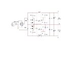
Does someone would be able to explain me how the current and voltage are distributing in the schematic ....

I tryed by myself for 2 hours, but I'm clueless it gives me impossible results. The center tap is confusing me and R1,R2 too...

It's bugging me because it's my final project at school and I don't fully understand the schematic and I'm supposed to be the best student of the class...

We passed 15 minutes studying the circuit and they allow us 5 hours to build it on a protoboard but nobody fully understand it.. that's stupid

5 hours to study it and 15 minutes to mount it would have been better!

Power supply 1.JPG
 
Last edited:

We passed 15 minutes studying the circuit and they allow us 5 hours to build it on a protoboard but nobody fully understand it.. that's stupid

5 hours to study it and 15 minutes to mount it would have been better!
Indeed! By the way: attachment link broken :?: Edit: I see link is fixed, but where it says "15V" you should read "0V" since you're using this as ground. AND: 15V AC != 15V DC. If you don't understand that, look up "alternating current"... concept of AC & how voltages / currents vary in time, is essential in understanding a circuit like this (blue line marked "pulsating" is what you'd expect as voltage across the 1000uF capacitors).

Does someone would be able to explain me how the current and voltage are distributing in the schematic ....
I'll bite:
  1. Transformer center tap serves as 0V reference point, all voltages are measured relative to this, most currents will use this as return wire.
  2. During 1 half of AC sine wave, current flows through one half of the transformer winding, 1 diode in the rectifier bridge, and upper 1000uF capacitor, charging capacitor to (approximately) 15V * SQR(2) - diode voltage drop = some 20V DC voltage? During other half of AC sine wave, same happens but through another diode in rectifier bridge.
  3. LM317 will allow current to pass from unregulated input to +Vo, in whatever amount (up to 1.5A or until LM317 gets too hot) is needed to maintain 1.25V between +Vo and LM317's "Adj" pin. R3 + variable resistor 'translate' this into a regulated +Vo voltage, see LM317 datasheet for the formula used. Series diode section 'messes up' ;-) this formula.
  4. Output current flows through load (RL2, 330 Ohm is pretty light load). This current (in combination with AC input) causes charging/discharging of the 1000uF capacitor, which in turns causes voltage across the capacitor to fluctuate (=ripple voltage). Heavier load (RL2 lower) -> larger ripple voltage.
  5. Same story as in 2-4 goes for LM337 half of the circuit, but with reversed polarities.
  6. The smaller 1 uF / 10 uF capacitors serve to suppress high-frequency noise in input voltages/currents. Important but otherwise not interesting for how the circuit works.
 
Last edited:

AND: 15V AC != 15V DC.

Yeah Retrotechie your right on that it's 15Vrms ,but the 1000uF cap will charge at Vpeak, so 15Vrms/.707 = 21.2 Vpeak
21.2V-.7V = 20.5V D.C.


By the way: attachment link broken

What you mean?

Thanks for your explanation

Gauthier
 

how did u solved this ? i saw title marked "solved"
disconnect center tap , connect GND to Earth AC wire. might help
 
Last edited:

Status
Not open for further replies.

Part and Inventory Search

Welcome to EDABoard.com

Sponsor

Back
Top