Continue to Site

Welcome to EDAboard.com

Welcome to our site! EDAboard.com is an international Electronics Discussion Forum focused on EDA software, circuits, schematics, books, theory, papers, asic, pld, 8051, DSP, Network, RF, Analog Design, PCB, Service Manuals... and a whole lot more! To participate you need to register. Registration is free. Click here to register now.

Need help for crosstalk problem

Status
Not open for further replies.

meeyaw

Junior Member level 3
Joined
Nov 29, 2010
Messages
26
Helped
0
Reputation
0
Reaction score
0
Trophy points
1,281
Visit site
Activity points
1,482
Hi edaboard people,

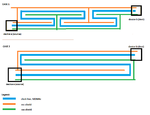
Please help me about this problem shown in the attachment image.
crosstalk problem.png

I have two possible routes for a clock line from device A to device B. As you can see, CASE A has more loop than case B. Both cases are shielded by vcc-vss pair.

The question is, which one is more prone to crosstalk: Case A or Case B? May I also know why is that so?

These cases confuses me already about which of them will I implement in layout.

Thanks for anyone who can answer it.
 

Although I can´t give an answer to the original question, my impression is that the 2nd option, due to have less breaks on path direction, depending on frequency range applyed, probably could be less susceptible to face problems related to reflection.
 

I don't believe that the "shield" stubs are helpful at all.

To a certain extent they can be helpful against crosstalk to adjacent signal routes at the same layer, not so much, however, against crosstalk to adjacent signal routes on layers below or above. In such case the screening could be extended to (virtual) GND layers above and below the clock line, which - on the other hand - increases the clock load capacitance quite a lot.

Another approach of course is to keep sensitive signal routes sufficiently far away, or - if necessary - cross with 2 differential mode signals, concerns sender or receiver.
 

Although I can´t give an answer to the original question, my impression is that the 2nd option, due to have less breaks on path direction, depending on frequency range applyed, probably could be less susceptible to face problems related to reflection.

@andre_tempron
Does less breaks in paths means less susceptible to coupling/reflection?

Other help needed: How can I translate it to a circuit model to have a simulation for both cases?
Thank you very much.
 

IC layout is a three-dimensional thing and it's more or less useless to discuss the effect of specific structures without knowing the complete geometry, how many metal layers, what's below (and possibly above) the shown traces.

Antenna-like shields can work at lower frequencies, at higher frequencies their series inductance must be considered in analysis. Similarly the effect of trace bends is frequency dependant.

It would be also helpful to know the purpose of the line meanders. Is it intended as delay line respectively delay compensation? What are the load and source impedances.
 

Hi,

The meanders are intended to add delay on the given path in the layout. The two devices are buffer circuits, parasitic RC being extracted. The line and vcc and vss shield are on the same metal layer, say M4, and the meander clock line is about 400um long (including the bends), 0.3um wide with spacing to its shield lines of 0.3u also.

I want to know by that two implementation which of the two is better in terms of crosstalk, and also want to know to create a SPICE model for the two implementation.
 

I guess, I should figure it out on my own. Thanks for the answers.
 

Status
Not open for further replies.

Part and Inventory Search

Welcome to EDABoard.com

Sponsor

Back
Top