WidElectronics
Newbie level 6

- Joined
- Aug 27, 2013
- Messages
- 14
- Helped
- 2
- Reputation
- 4
- Reaction score
- 2
- Trophy points
- 3
- Location
- Bangalore, INDIA
- Activity points
- 97
Hi all,

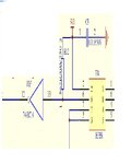
Above I have attached an image of the circuit.. Any one plz guide about its operation....:?:
HFBR is a transceiver and ic name is not given...
U1F is 7414 ic- hex inverter ic...
In HFBR pin no.1-RO(receiver o/p), 2-(RE-active low), 3-DE(data enable), 4-DI(data i/p), 5-gnd,6-A/Y(it is input if DE=0, o/p if DE=1)noninverting receiver i/p or driver o/p,
7-B/Z( same as A/Y but inverting),
8-Vcc
Hoping for solution...:grin:
Thanks in advance
Last edited:
