Continue to Site

Welcome to EDAboard.com

Welcome to our site! EDAboard.com is an international Electronics Discussion Forum focused on EDA software, circuits, schematics, books, theory, papers, asic, pld, 8051, DSP, Network, RF, Analog Design, PCB, Service Manuals... and a whole lot more! To participate you need to register. Registration is free. Click here to register now.

[Moved]: Improving glitch from DAC circuit

Status
Not open for further replies.

AfiqahRS

Newbie level 3
Joined
Jan 22, 2017
Messages
4
Helped
0
Reputation
0
Reaction score
0
Trophy points
1
Activity points
42
Hi,

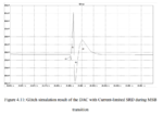
How can I improve glitches encountered on following DAC circuit? I have implemented an SRD (Swing Reduced Driver) to the circuit but somehow I need to reduce another 5% of these glitches. Any simple method that can be implemented? I have attached the circuit as well.

View attachment Schematic of Hybrid DAC.rar
 

Re: Improving glitch from DAC circuit

It would be reasonable to add a few words of specification and analysis, e.g.:
- specification of your DAC (speed, resolution, supply voltage, output signal level)
- what's the observed glitch level
- how does it compare with industry standard DACs
- can you locate the main cause of glitches
 

Re: Improving glitch from DAC circuit

Dac specification:
voltage references: 735.127mv
Vdd:1.1v
Sampling frequency:100MHz
Offset error:16.06mv
Current glitch energy:17.4122pVs
For this circuit the glitches is due to the binary weighted resistor string and switchable current source. Is there anyway to improve switchable current source to ensure signal are not overlapping? Or is there any better approach to improve these glitches?
Capture.PNGCapture1.PNGCapture3.PNGCapture4.PNG
 

Re: Improving glitch from DAC circuit

Not knowing how the DAC is architected, maybe these
suggestions are off base. However...

1) If your weighted resistor string is switched into the
output, put the resistor between the output and the
switch, to better isolate its charge injection

2) Switches to be no larger than necessary, and driven
no harder than necessary

3) If a current-mode into @-2R ladder style, switch the
currents by source-steering rather than drain switching.

4) Output capacitance will smooth out current spikes, at
the potential cost of settling time. Be sure you have
the load and parasitics represented well, before you
get all sad (or happy) about DAC glitch qualities. A
post-filter could be something to consider (series L
smooths current, shunt C smooths voltage, the two
together can make a nasty little tank).

Now, your glitch energy spec seems wrong. Calling out V*s
is not specifying an energy quantity, unless you have an
assumed load embedded in that number. V*I*s is energy.
V^2/R*s is energy.

If you showed a DAC bit cell and ladder schematic some
other ideas might occur to people. Topology suggestions
(useful ones) need some initial context.
 

Re: Improving glitch from DAC circuit

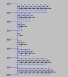
My circuit is a 12 hybrid of a thermometer DAC and Binary weighted resistor string. 8 bit from the binary weighted resistor string, 4 bit from the thermometer. Here are my binary weighted resistor string circuit and switchable current source circuit. As for the switchable current sources is there a better way to improve it? I have attached my circuit as well on the first post.

pic1.PNG
pic2.PNG
Pic3.PNG
 

Re: Improving glitch from DAC circuit

I once built a binary-weighted resistor DAC. I also got glitchy output like you. I could not interpret which resistor was off-spec, so I resorted to installing 8 potentiometers instead. I adjusted each one until I saw a smooth slope.

The resistance values need to be compatible with resistance in neighboring components.
The LSB cannot have too high a resistance, and the MSB cannot have too low resistance.

Is your digital count in binary or BCD? When I tried BCD chips, it worked but I found there needed to be an odd jump in resistance between two IC's, since the count skipped A through F. This made the potentiometer setup almost a necessity for BCD.
 

Re: Improving glitch from DAC circuit

You should size-weight the current switches the same
way as you do their resistors. Begin with a minimum-W
one at the LSB and increment by octaves.

You might benefit by putting a grounded-gate PMOS,
supply-gate NMOS cascode between each real switch
P and N device and the ladder nodes, this will shunt a
lot of glitch energy from the switch gates into the supply
rails instead of the output.

.rar files require particular compression tools and are
not handled by many of the more common ones, so I
am not looking at your Post#1 schematic.
 

Status
Not open for further replies.

Similar threads

Part and Inventory Search

Welcome to EDABoard.com

Sponsor

Back
Top