Continue to Site

Welcome to EDAboard.com

Welcome to our site! EDAboard.com is an international Electronics Discussion Forum focused on EDA software, circuits, schematics, books, theory, papers, asic, pld, 8051, DSP, Network, RF, Analog Design, PCB, Service Manuals... and a whole lot more! To participate you need to register. Registration is free. Click here to register now.

MOS Enclosed Gate Layout

Status
Not open for further replies.

Tbit

Newbie level 3
Joined
May 13, 2007
Messages
4
Helped
0
Reputation
0
Reaction score
0
Trophy points
1,281
Activity points
1,316
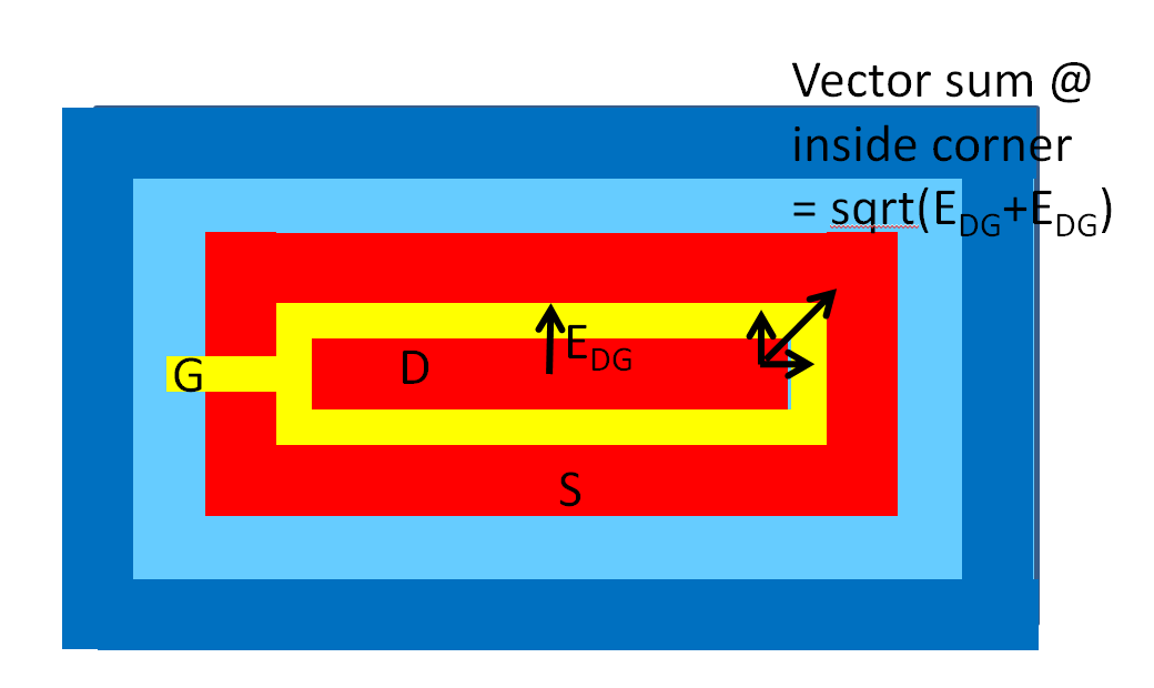
The enclosed gate layout (ELT)of a MOS transistor is a popular physical implementation in mitigating the effects of TID (ionising radiation) on normal device operation in Space/Cosmic environments.

A couple of questions:

1/ I would appreciate knowing where I can find detailed classic information on the principle of the MOS enclosed gate layout structure to mitigate TID effects?

2/ If the modelling of this ELT structure is accounted for in any BSIM/Compact Spice model then what are the parameters involved and how do they differ from the BSIM model of a normal MOS transistor layout?
 

In the industry this tends to be more "art in pocket" than
documented science. You will however find discussion of
it in various papers from IEEE NPSS society, especially the
NSREC conference publications and IEEE TNS. Which of course
the Irrelevant Ensemble would prefer you pay for while they
provide nothing back to the authors.

You will probably also find papers, and more accessible,
from ESA and CERN researchers.

The basic principle is, in junction-isolated or partially-depleted
SOI, that excess leakage and other gate-kink type misbehavior
comes from the bird's beak (LOCOS) or trench affected edges
of the active gate. So if you eliminate the edge you eliminate
the (or, that) problem.

Not to say you won't accrue others. For example, a common
annular gate geometry is drain inside, source outside. This is
best for speed and drive (minimize Cdb and Cdg, minimize Rs)
but you also then impose a 40% higher peak drain-gate field
at the inside corners (vector sum in the spacer oxide) which
may well violate the qualification paradigm of the foundry
and give you HCE you did not expect (but this, synergistic
HCE*radiation effects, is something that you ought to be
looking at yourself anyway).

Modeling is a little tricky as regards the true W, especially
as gate length increases (the channel becoming sort of
trapezoidal-donut, W at one end != W at the other end).
You can probably find formulae but they bear verifying
in silicon. You will change AS, AD, PS, PD and this can
be calculated from layout dimension pick-offs. This is
not about the compact model; it's just parameterization.

In FDSOI the annular gate may not help you, because
the back interface is not really under front-gate control
under a large range of bias conditions.
 
  • Like
Reactions: Tbit and erikl

    erikl

    Points: 2
    Helpful Answer Positive Rating

    Tbit

    Points: 2
    Helpful Answer Positive Rating
In the industry this tends to be more "art in pocket" than
documented science. You will however find discussion of
it in various papers from IEEE NPSS society, especially the
NSREC conference publications and IEEE TNS. Which of course
the Irrelevant Ensemble would prefer you pay for while they
provide nothing back to the authors.

You will probably also find papers, and more accessible,
from ESA and CERN researchers.

The basic principle is, in junction-isolated or partially-depleted
SOI, that excess leakage and other gate-kink type misbehavior
comes from the bird's beak (LOCOS) or trench affected edges
of the active gate. So if you eliminate the edge you eliminate
the (or, that) problem.

Not to say you won't accrue others. For example, a common
annular gate geometry is drain inside, source outside. This is
best for speed and drive (minimize Cdb and Cdg, minimize Rs)
but you also then impose a 40% higher peak drain-gate field
at the inside corners (vector sum in the spacer oxide) which
may well violate the qualification paradigm of the foundry
and give you HCE you did not expect (but this, synergistic
HCE*radiation effects, is something that you ought to be
looking at yourself anyway).

Modeling is a little tricky as regards the true W, especially
as gate length increases (the channel becoming sort of
trapezoidal-donut, W at one end != W at the other end).
You can probably find formulae but they bear verifying
in silicon. You will change AS, AD, PS, PD and this can
be calculated from layout dimension pick-offs. This is
not about the compact model; it's just parameterization.

In FDSOI the annular gate may not help you, because
the back interface is not really under front-gate control
under a large range of bias conditions.

@dick_freebird, Thanks for this information, it is good to have a perspective on this matter that throws up further light. I found it particularly elusive to extract the primary factors involved in developing practical MOS radiation hardness methodologies. I have been wondering what kind of 'black-art' this is that I have stumbled upon, and further complicated by the complimentary/negating TID attributes of Ultra DSM CMOS/FD-SOI. As kindly suggested, I will try and find what I can from ESA/CERN research material.
I would appreciate if you could elaborate further on the 40% figure for peak Drain-Gate electric field for the annular geometry ELT. I scratched my head a few times when you stated these exacting figures.
 

+40% is really *sqrt(2) - vector sum of the two orthogonal
D-G fields close-in to the edge. Like the flip side of how
you want a spherical end to your Van De Graf tower, the
local curvature affects breakdown. You could mitigate this
by (say) 45-ing the gate corners, but in newer nodes this
(non-manhattan) geometry may be verboten.


Status
Not open for further replies.

Part and Inventory Search

Welcome to EDABoard.com

Sponsor

Back
Top