Continue to Site

Welcome to EDAboard.com

Welcome to our site! EDAboard.com is an international Electronics Discussion Forum focused on EDA software, circuits, schematics, books, theory, papers, asic, pld, 8051, DSP, Network, RF, Analog Design, PCB, Service Manuals... and a whole lot more! To participate you need to register. Registration is free. Click here to register now.

mos diode(G,D short connected) recover time!

Status
Not open for further replies.

nelly1

Junior Member level 3
Joined
Jun 14, 2012
Messages
29
Helped
0
Reputation
0
Reaction score
0
Trophy points
1,281
Visit site
Activity points
1,495
Hello everyone,

Does mos diode also has forward and reverse recover time? I know the body diode has, but what about the whole mos diode?

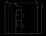
when i used mos diode as normal PN diode in a buck converter, I saw a current which looks like a "reverse recovery current" though my mos diode like picture shows below. So i wonder if this happens because the depletion capacitances need to discharge.

Please give me some reference about mos diode!!!!It's reallllly hard to find useful information in internet.
thanks a lot!
mos diode.jpg
 

When you say MOS diode are you referring to the diode formed by the drain-bulk PN junction, or something else? Technically MOS diode is a term for a MIS structure which behaves like a variable capacitor, not a diode...
 

i mean the mosfet whose Gate and Drain are shorted and it's I-V curve looks the same like a diode...
 

Okay, that's a good question. A MOS channel is a majority carrier device, so I would assume there's no reverse recovery. But I'm not sure what happens to excess majority carriers in the channel when the channel is suddenly depleted (and those carriers would suddenly become minority carriers if they still exist). But looking at your waveform, it looks like the small spikes could definitely be due to junction capacitance, not recovery effects. Very hard to know for sure though.
 

thanks for your answer! when u say the spike is due to junction capacitance, how to improve it? it happens on the diode(mos acts as diode) when the swtich from off to on state.
And i m also confused about the discharging trace of the junction capacitance. Does it discharge through the output load or???
mos diode schematic.png
 

Status
Not open for further replies.

Similar threads

Part and Inventory Search

Welcome to EDABoard.com

Sponsor

Back
Top