Continue to Site

Welcome to EDAboard.com

Welcome to our site! EDAboard.com is an international Electronics Discussion Forum focused on EDA software, circuits, schematics, books, theory, papers, asic, pld, 8051, DSP, Network, RF, Analog Design, PCB, Service Manuals... and a whole lot more! To participate you need to register. Registration is free. Click here to register now.

ML4800 will not reduce ripple in PFC output caps?

Status
Not open for further replies.

cupoftea

Advanced Member level 5
Joined
Jun 13, 2021
Messages
2,611
Helped
54
Reputation
108
Reaction score
115
Trophy points
63
Activity points
13,685
Hi,
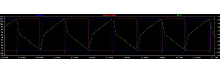
We have a 1kW Boost PFC followed by a Half Bridge. They are both driven by a ML4800 controller. The PFC is leading edge driven. That means, the PFC diode will conduct just as the Half bridge FET turns ON…..the problem is, our half bridge uses the transformer leakage inductor as the “output inductor”. As such, its waveforms are as attached (primary current and both FET gate drives). This shows that the ML4800 principle of reducing ripple in the PFC output caps simply doesn’t work for us….would you agree?

ML4800
 

Attachments

  • Half Bridge Waveforms from ML4800.jpg
    Half Bridge Waveforms from ML4800.jpg
    114.4 KB · Views: 90

Thanks,...i do apologise...........my mistake, the PFC is driven by the ML4800 at 100kHz, the Half Bridge is driven by a L5991 which is synced by the ML4800 PWM O/P pulses.

There is a Flip flop to allow the L5991 to produce the requisite drive pulses for the half bridge.

So both PFC, and Half Bridge operate at 100kHz....
 

O.K., in this case we can only guess about the actual current waveforms. Regarding ML4800 reduced ripple claim, pfc DC ripple is 100 Hz modulated, pwm input ripple almost constant, so we can at best reduce the average and maximum ripple by a certain amount. Good if it comes for free, but probably not worth a considerable BOM enlargement.
 
O.K., in this case we can only guess about the actual current waveforms.
Thanks,
The L5991 (our half bridge driver) is set up as a "slave", and receives a sync pulse (which gets divided down) from the ML4800 PWM O/P pin. When L5991 receives this sync pulse, it terminates its PWM cycle. The ML4800 sends the PWM O/P pulse just as the PFC diode is about to conduct. So in other words, the PFC diode "pulse" of current, does not line up with the maximum current point of the Half Bridge primary. As such, there is no benefit in terms of reduced ripple current in the PFC output capacitors, i believe this to be correct?
Waveforms of Half Bridge are as shown in top post (Primary current, both gate drives)
L5991 datasheet
 

The effectiveness varies with load and position along the mains half cycle,

the PWM in the booster is not constant - so the matching to the o/p stage is not perfect except at a few spots along the half sine, for some engineers, some reduction in power stage current ripple in the electrolytics is desire-able ....
 
Thanks, i see what you mean, but in the above case, the switch on of the PWM stage happens, all the time, (wherever in the mains half cycle) at the very worst place....ie, just as the PFC boost diode starts conducting. (please see waveforms in top post of the PWM stage primary current and half bridge FET gates).
So the ripple is worse than if no synchronisation had been done at all.

In other words, the way that i am saying , maximises the ripple current in the PFC output caps....looking at the waveforms of the top post and you can see this......the L5991 turns on its gate when it receives the high going sync pulse....ML4800 turns on the boost diode just as the PWM O/P goes high.....(the PWM O/P pulse is used to sync the L5991)

So I am just wondering how they have managed to do this......maximising the badness......
 

there is an error in your analysis
Thanks,
I am taking it that for ML4800, the PWM O/P goes high at the instant that the PFC diode starts conducting.
I am also taking it that the L5991's Gate drive goes high, when the incoming Sync pulse goes high.

....If the above is correct, then my analysis is correct. (please remember that we are not doing a "standard" half bridge....ours has no output inductor, just the leakage inductor)

...indeed, if we were doing a "standard" half bridge converter (ie in deep CCM with an output inductor).....then the ripple current in the PFC output caps would indeed be reduced, and everything would be good....its the fact that we are doing a "leakage inductor based half bridge", that means the ML4800 syncing the L5991 actually makes the ripple in the PFC output caps as bad as it can be.......this can be seen partly by examining the waveforms of the top post.
 
Last edited:

sigh, when the boost "diode" is on, current is flowing into the boost electro's, however if we also have a switch ON for the down converter, then the current also goes into the o/p stage, hence the net current in the boost electro's is reduced by that amount which goes to the output stage,

similarly, when the boost mosfet is on, there is no current in the boost diode, and - if in synch - no current in the down converter switches as they are off, of course, for a typical booster there is not perfect alignment except for a few points or regions on the mains half cycle ....
Thanks, i totally agree, and you are stating the "normal" correct action of the ML4800. I do appreciate i am indeed asking too much to ask people to get in to my particular situation.....the situation i have does not correspond to the "normal" one.....if you look at the waveforms in the top post, you can see what i mean......these are not "normal" half bridge SMPS waveforms......the FETs are on maximum duty, and the primary current builds up to maximum long after switch on......its a totally different primary current waveshape than a "normal" half bridge.....and so the normal ML4800 regime does not reduce capacitor ripple current on this case.
This is a half bridge smps with no output inductor, and the fet duty is maximum all the time. Its an open loop half bridge with no output inductor. (uses Leakage L)

To achieve ripple reduction in this case, the pfc diode oncoming would need to correspond to the half period point of the Half bridge...then the boost diode conduction would always basically sync up with the half bridge primary current maximum.
 

Its just that i cant believe they got this wrong.......so i am seeking the reality check......ie, please to look at the waveforms in the top post, and ask yourself, where would you want the boost diode to start conducting in order to reduce capacitor ripple current.?.........i am sure you would agree.....you would not want the start of pfc diode conduction to correspond with the fet switch on instant....

The waveforms show both fet gates, and primary current, of the "abnormal" half bridge smps.
 

You are right, the diagram contains the claimed pwm waveforms, but I was expecting a combined display of pfc and pwm waveforms to check for the synchronicity problem.
 
You are right, the diagram contains the claimed pwm waveforms, but I was expecting a combined display of pfc and pwm waveforms to check for the synchronicity problem.
Thanks, sorry i have not posted that.....it will take some time to make up and run the sim for that. -And in fact, you can actually see all you need from the waveforms in top post........just imagine the pfc diode current starting at the instant that each gate goes high.

You can actually tell that the pfc diode current conduction would best start at the middle of the fet on time...the fets are always on max duty cycle. There is no feedback loop....just overcurrent limitation.

I attach here the Half Bridge SMPS PDF and LTspice
 

Attachments

  • Half Bridge SMPS.pdf
    181.3 KB · Views: 95
  • HALF BRIDGE SMPS.zip
    3.5 KB · Views: 63
Last edited:

even for so called "normal" 1/2 bridge operation there is limited ripple reduction in the DC bus caps - due to the time varying current in the boost choke, i.e. zero to 2x Iave ( 1.414 x Irms )
--- Updated ---

conversely - if the following converter is an half bridge running at near full pwm, then any ripple reduction that is going will be had, as there is always a current path thru the down converter to the output ( assuming constant load )

remember that usually, most of the Imag locked up in the Tx every 1/2 cycle is returned to the pri side.
 
Last edited:
conversely - if the following converter is an half bridge running at near full pwm, then any ripple reduction that is going will be had, as there is always a current path thru the down converter to the output ( assuming constant load )
Thanks, would you agree that in this case, no sync up at all, would be better than what is now given...or at least, just as good as?.....ie just let down_converter and pfc operate freely at 100khz.
 

Status
Not open for further replies.

Part and Inventory Search

Welcome to EDABoard.com

Sponsor

Back
Top