Continue to Site

Welcome to EDAboard.com

Welcome to our site! EDAboard.com is an international Electronics Discussion Forum focused on EDA software, circuits, schematics, books, theory, papers, asic, pld, 8051, DSP, Network, RF, Analog Design, PCB, Service Manuals... and a whole lot more! To participate you need to register. Registration is free. Click here to register now.

[SOLVED] Minimizing RF radiations and leakages, shielding 3-stage 90dB RF Attenuator

Status
Not open for further replies.

cjrathi

Member level 2
Member level 2
Joined
Oct 18, 2012
Messages
52
Helped
0
Reputation
0
Reaction score
0
Trophy points
1,286
Visit site
Activity points
1,704
Hi,

I have designed 90dB RF Attenuator using three Peregrine PE43703 30dB parts.

This design has been enclosed in a metal case (snapshot attached). Hence body mount SMA connectors are used for input and output.

As seen in the snapshot, all three stages are getting shielded by the metal compartment. Shielding from top has been achieved from the lids on top tightly screwed.

This design works fine till 90dB attenuation in 2-3 GHz range giving good step linearity. But I am facing issues in 5-6 GHz band.

Issues are:-

When stage 1 and 3 are set to full attenuation (60dB), it works fine. But when stage 1 and 2 are set, there is linearity issues in 5-6 GHz. i.e., setting 60 dB attenuation, total attenuation at 5.15GHz, 5.5GHz and 5.85Ghz are 67dB, 67dB and 68.1dB (considering 7dB insertion loss in this range). At 5.85GHz freq, ideally it should be also 67dB.
After this, keeping 1st and 2nd stage to full attenuation, when 3rd stage is varied from 0 to 30dB, this non-linearity is increased giving drastic degradation in S21 even at 5.15GHz and 5.5Ghz freq.

As per my study, the issue could be:-

1. Signal is getting leaked somewhere from RF path.
2. There could be an impedance mismatch of RF trace below the tunnel. (??)
3. Possibility of forming a waveguide/resonant box which is leaking the signal from input to output. (??)
4. Stage to stage coupling through ground planes (??)
5. Leakage through body mount SMA connector (??)

Please suggest the reason of this issue and possible solution to minimize those effects..

Thanks,
CR
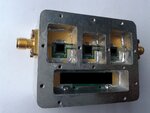

20130929_160405.jpg
 

Your design looks good but you have not indicated the input power levels possibly causing the linearity problem.
Concernng the SMA connectors, try to solder them to the case or use silver epoxy to seal ground connection.

In high-loss attenuators like yours always test the driver lines for the leakage. Sealing the lid is also important. Resonance of the cavity can be suppressed by lossy fom glued to the lid.

How do you calibrate the loss? I would suggest to try a good spectrum analyzer which can be calibrated from 0 to -80 dBm while the input power to your attenuator is kept under the specified linear input power.

- - - Updated - - -

Also make sure you use good (best semirigid) cables. Even a tight SMA connector leak is close to 90 dB.
 
Hi--

Input power level is well within chip specs.

I have already tried to contain the leakage of SMA connector by proper soldering, even outside the box at the panel, but still no improvement.

I guess lid is also sealed very tightly. But still I soldered all three cavities from top with thin copper plates. Yet it didn't improve the performance.

I even minimized the tunnel size by soldering copper plate, as it looked very large may be not satisfying coplanar TL characteristic and causing stage to stage leakage. Still there is no effect.

I have already tested this design with PCB edge mount SMA connector and shielding via thin copper plates (i.e., not like shielding extruded in the box). And it gave nice linear 90dB attenuation in 5GHz band too.

Is it the case design that is causing an issue? Because only difference bet this and prev design is SMA connector and shielding technique.

I am using good calibrated NA for testing. Same setup is used for prev working design too. So I don't think this could be an issue.

I am planning to repeat the same process in another case with same structure and see whether same performance is getting repeated.

Could you suggest something else?

>>CR
 

In the photograph I do not see the control lines and how they are RF-blocked. I can see that the via holes are not many with wide gaps between them, I can guess not closer than 0.15".The behavior of the attenuator you write is good below 5 GHz but worse above.
I would try driving line sensitivity below 4 GHz with open cavities, also filling the cavities above the chips with a lossy foam.
Achieving 0-90 dB at >5 GHz is often tricky like in your case. With a patience you will find the weak points and get a good result.
 
RF blocking CAPs for control signals are at the bottom side. As far as no. of vias/ vias spacing is concerned, it is as per the working design.

I tested newer board in another case with 1mm compartment width of small tunnel size. Getting same performance.

It seems - There is no issue with tunnel size and compartment width.

The results start degrading as soon as 2 adjacent stages are ON. That means I guess there is an stage to stage leakage. I don't know how.

I think ---

1. There must be input to output leakage within each stage

2. The sizes of three cavity being different causing any issue. Is it possible that if three cavity sizes for three stages, if different, affects the frequency response?

3. Are DC blocking caps between each stages causing this issue? Caps used are RF.

4. Is this because RF connector is not getting good ground connection? Right now as it is panel mount SMA, it is getting ground via case body, which is supposed to be long return current path. In earlier working design, we used edge mount SMA.

5. Is it because, stage to stage distance is more for 5GHz (which is 6mm). In earlier working design it was very less 3mm.

What do you think could be the reason???

>>CR
 

As your device is good to some 3-4 GHz but not above, try other capacitors. Many SMD capacitors resonate above 4 GHz. Connect 1 nF capacitors in parallel with installed ones and see if the response changed.
 
Please suggest the reason of this issue and possible solution to minimize those effects..
How about absorbers in a sections. Dimension of the sections are same with λ/4. Of course capacitors should be broadband. And VIA s as well good. But absorbers, it necessary.
 

How about absorbers in a sections. Dimension of the sections are same with λ/4. Of course capacitors should be broadband. And VIA s as well good. But absorbers, it necessary.

I will try to retest with RF absorbers. But will have to use conductive adhesive . Right ?

What does section to be lambda/4 mean exactly?

>>CR

- - - Updated - - -

As your device is good to some 3-4 GHz but not above, try other capacitors. Many SMD capacitors resonate above 4 GHz. Connect 1 nF capacitors in parallel with installed ones and see if the response changed.

Okay I will try that. Right now I am using series RF Cap of 5.6pF.

I even removed those RF Caps and shorted them using solder and surprisingly there was no change in the response. Do you think this RF Caps value/characteristics causing issue?

Could you suggest you alternate values/ options?

<<CR
 

I will try to retest with RF absorbers. But will have to use conductive adhesive . Right ?
>>CR
No
What does section to be lambda/4 mean exactly?
cavity works like resonator and as result big coupling input -output. And probably trough pow supl lines filters doesn't works any more. Complex EMC
problem.
 

No

cavity works like resonator and as result big coupling input -output. And probably trough pow supl lines filters doesn't works any more. Complex EMC
problem.

So is it okay to just keep the absorber within the cavity?


Is it necessary to keep cavity length lamda/4? What should we consider f for lamda? Max operating f?

>>CR
 

So is it okay to just keep the absorber within the cavity?
>>CR
May be directly to the chip, may be to the walls of your cavity. You see at 2GHz it works. @2GHz here λ is 100mm ( of course bandwith should be valid for these chip !I`d never check) but for 5GHz it`s ~ 50-60mm.
Do you see differences? Of course there could be different effects as well.
Is it necessary to keep cavity length fell? What should we consider f for lamda/4? Max operating f?
Yes. length lamda/4 is 10-15mm. I made such antennas. Really cavity should be less than lamda/8-10 or with absorber.
And accurate with VIAs @ 6GHz. I made in one case 0.3mm but they didn't work like VIAs.
 
Last edited:

90 dB separates the men from the boys! You need to cowboy up.

Are there lowpass filters on EVERY WIRE that comes into each of those three cavities?

Is there absorber material (like eccosorb) on the not-shown cover?

Why are there so few holes holding the cover to the housing. Add around 20 more tapped holes.

Are you using SMA connectors that are rated for 90 dB leakage? Some have little holes in the side with glue that leak out.

What about that big long cavity (i.e. nice waveguide leakage path) along one side. What are you doing to stop a frequency resonance in that huge cavity?

Why are the three cavities holding the circuits so big? Could u not shrink them down, especially the height? Look up "box resonances".

It might be just chip to chip vswr interaction causing your "non linearity". Do those chips, by themselves, hold at least 15 dB return loss over their attenuation range? (25 dB would be better!)
 
Hi ....

Thanks for your all suggestion.

The actual issue have been found out... Actually there was stage to stage coupling through the substrate itself.. We isolated each stages by cutting the board except at RF trace section... and guess what it worked linearly even after 60dB attenuation.. :)

>>CR
 

Interesting, could you show a picture of the results? What is the make and thickness of the substrate?

I'm surprised the substrate could couple the signal itself, maybe you just needed a dense via fence around the border of each cavity?
 

I had a line of 140 MHz if amp modules, with saw filters in them. We ended up punching out a rectangular hole under the saw filter can for just this reason....stuff was propagating under the saw filter.
 

PCB Material used is Rogers+FR. Thickness is 2mm. It seems the power level is so low that it starts coupling through substrate itself after 60dB. Even just via fencing wouldn't have worked for full 90dB range. It needed full isolation thr cuts.

Actually our prev working design all had cut and it was working fr full range, but we never thought this design will have this issue.

>>CR
 

PCB Material used is Rogers+FR. Thickness is 2mm. It seems the power level is so low that it starts coupling through substrate itself after 60dB.

>>CR
I never know concerning these piece of art. 2 mm with ξ » than 4 it works like waveguide @ those frequencies. Absorbers and right VIAs could be useful as well for final iteration.
 

I never know concerning these piece of art. 2 mm with ξ » than 4 it works like waveguide @ those frequencies. Absorbers and right VIAs could be useful as well for final iteration.

Overall PCB thickness is 2mm. Top layer Rogers thickness is 10mils. Rest h is FR4. We did 2mm overall thickness for design purpose.

>>CR
 

Status
Not open for further replies.

Similar threads

Part and Inventory Search

Welcome to EDABoard.com

Sponsor

Back
Top