Continue to Site

Welcome to EDAboard.com

Welcome to our site! EDAboard.com is an international Electronics Discussion Forum focused on EDA software, circuits, schematics, books, theory, papers, asic, pld, 8051, DSP, Network, RF, Analog Design, PCB, Service Manuals... and a whole lot more! To participate you need to register. Registration is free. Click here to register now.

Measuring the impedance of my circular loop antenna

Status
Not open for further replies.

doenisz

Junior Member level 1
Joined
Sep 12, 2021
Messages
17
Helped
0
Reputation
0
Reaction score
0
Trophy points
1
Activity points
258
Hi everyone,

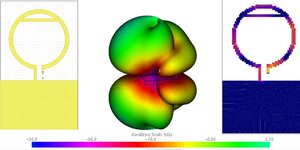
I am trying to measure the impedance of my circular loop antenna at 3.5GHz. It is heavily inductive, with my HFSS simulations giving its impedance as around 6+j280 at 3.5GHz.

Here is how it looks like, there is soldermask exclude around it:

1664310065071.png


There is no ground plane on this PCB, as it kills the radiation of this antenna. It is on FR4 substrate, which, I know is lossy, but this is just a prototype, I will pass to low-loss RF substrates (like Rogers) in the actual implementation.

My question is that, I have just measured the S-parameters of this with a network analyzer that has a probe station. Its probes are -unlike my antenna- signal and ground and not differential. I just physically touch the signal probe to one terminal and ground to other.

Basically, I observed very similar reactance to my simulations, but the resistance (real part) turned out to be 70 ohms, which is SEVERELY off from the simulations.

Is there anything wrong with my approach? I asked this question on Reddit too, and someone recommended using a Balun to convert from single-ended to differential signaling. He also mentioned "chassis" which I have no idea about? ( )
In the HFSS simulations, I just use a lumped-port, I have no idea if it is differential or single-ended, nor if it's the cause of my problems for the huge resistance discrepancy.

How should I go about taking more accurate measurements?

Thanks for any help.
 

In the HFSS simulations, I just use a lumped-port, I have no idea if it is differential or single-ended
The lumped port in simulation behaves like a differential port here, so that part is fine.

Your measurement probe has much "ground" metal, so it loads the two terminals in an non-symmetric way. This can certainly affect the antenna, but I would expect a change in inductance rather than extra loss. Did you include copper loss and FR4 dielectric loss in your HFSS model? For FR4 at 3 GHz I would use tand=0.03.

Balun: When I created a small 915 MHz loop some years ago, I used a lumped element balun to connect the symmetric antenna to the non-symmetric coax feedline. Without the balun, the antenna was easily detuned and "hand sensitive", the coax became part of the radiating structure.
 

    doenisz

    Points: 2
    Helpful Answer Positive Rating
The lumped port in simulation behaves like a differential port here, so that part is fine.
Is there a way to simulate with the unbalanced/single-ended signaling with HFSS? Like signal and ground? Matching that to the measurement is also fine.

This can certainly affect the antenna, but I would expect a change in inductance rather than extra loss. Did you include copper loss and FR4 dielectric loss in your HFSS model? For FR4 at 3 GHz I would use tand=0.03.
Why? I would expect that the inductance just comes from the loop-wire and is defined more from the geometry, so I was expecting to have it similar, which turned out to be true. I model the losses you mentioned. Used tand=0.02 though. Making it 0.03 probably won't jump the resistance from 6 ohms to 70 ohms.

Balun: When I created a small 915 MHz loop some years ago, I used a lumped element balun to connect the symmetric antenna to the non-symmetric coax feedline. Without the balun, the antenna was easily detuned and "hand sensitive", the coax became part of the radiating structure.
My feed is just a probe station and not coax/SMA, so I am inclining more towards just ordering a differential probe.
 

Is there a way to simulate with the unbalanced/single-ended signaling with HFSS? Like signal and ground? Matching that to the measurement is also fine.
It just depends what else you connect to the internal ports minus pin (reference). If you add the probe ground and other structures connected to the port reference, it becomes asymmetric and gives a better match to your hardware situation.
--- Updated ---

Why? I would expect that the inductance just comes from the loop-wire and is defined more from the geometry, so I was expecting to have it similar, which turned out to be true. I
Other conductors near the loop will change magnetic fields (don't penetrate much into conductors due to skin effect) and this will have some effect on loop inductance - if the other metal is close enough. Not sure about your probe body, you might want to add that (roughly) in your EM model and see how much it changes results.
--- Updated ---

I model the losses you mentioned. Used tand=0.02 though. Making it 0.03 probably won't jump the resistance from 6 ohms to 70 ohms.
I agree!
 
Last edited:

It just depends what else you connect to the internal ports minus pin (reference). If you add the probe ground and other structures connected to the port reference, it becomes asymmetric and gives a better match to your hardware situation.
Thanks for the info but I am not sure if I got it fully. In HFSS, I use a lumped port with an integration line. Is what you wrote for the measurement setup or HFSS? Isn't my measurement of signal/GND already asymmetric?
 

Thanks for the info but I am not sure if I got it fully. In HFSS, I use a lumped port with an integration line. Is what you wrote for the measurement setup or HFSS? Isn't my measurement of signal/GND already asymmetric?

I refer to simulation. Ground is a human concept, and in EM simulation there is no a-priori ground. Only if you have something like an extended ground plane in simulation, or a large PEC boundary that you connect as port reference, that behaves like a hardware ground plane because you connected it that way.

The reference terminal of an internal SIMULATION port is not connected to anything magic like "global ground", whereas in HARDWARE your probe tip ground is connected to other conductors (probe ground connected to probe body -> coax shield -> VNA chassis etc).

If you connect a lumped simulation port to a symmetric device, you get perfectly symmetric excitation.

To have similar situation in hardware and simulation, you can use a differential probe OR try to imitate in simulation your hardware scenario by adding nearby metal that is connected to probe ground.

Does this make sense?
 

    doenisz

    Points: 2
    Helpful Answer Positive Rating
To have similar situation in hardware and simulation, you can use a differential probe OR try to imitate in simulation your hardware scenario by adding nearby metal that is connected to probe ground.
Ok, so either the measurement will be balanced like the simulation; or the simulation will be unbalanced like the current measurement. Former is straightforward, though I never calibrated using differential probes.

As for the latter, here is how my port looks like now. There is no ground plane, I use a lumped port with the integration line as I said earlier, so based on your remark, it is symmetric/differential.

1664388087894.png


Let's say the left-side is signal and right-side (terminal) is GND. Practically, what do I do to imitate the measurement setup? If I add a PEC at the bottom of the PCB and make it reference, it's completely different than the measurement setup. Can you show on this figure what do I need to add?

Thanks.
 

One comment upfront: I suggest to place the port between the narrow feedline only, not across the entire width of the ring. Your hardware current needs to enter through the narrow feedline, so force simulation current to use that path as well. You will notice that resistance increases by enforcing that (realistic) current path.

Imitating probe ground: Add some more metal to one terminal (one side of your port/feed). I don't mean placing anything underneath the coil -- that's bad indeed! I suggest that you add something shaped like your probe body and connect that to one (!) of the port ends/feedlines. This will represent the true physical ground path that your probe has in measurement, and it will introduce an asymmetric load to the port.

I'm working on EM Modelling of on-chip structures at very high frequencies (up to 200 GHz) and can confirm that it is tricky to include proble-related effects. There are some guys at a Berlin research lab who had great success with modelling their probes in detail, including some coax and absorber inside the probe, but that would be overkill here at only 3.5 GHz. But it's certainly worth a try to add some basic probe "body" metal to your model and connect it at one side of the port.
 

    doenisz

    Points: 2
    Helpful Answer Positive Rating
One comment upfront: I suggest to place the port between the narrow feedline only, not across the entire width of the ring. Your hardware current needs to enter through the narrow feedline, so force simulation current to use that path as well. You will notice that resistance increases by enforcing that (realistic) current path.

Imitating probe ground: Add some more metal to one terminal (one side of your port/feed). I don't mean placing anything underneath the coil -- that's bad indeed! I suggest that you add something shaped like your probe body and connect that to one (!) of the port ends/feedlines. This will represent the true physical ground path that your probe has in measurement, and it will introduce an asymmetric load to the port.

1664394356112.png

Applied your suggestions. Narrowing the port did not change much but changing the right-hand side of the feed much longer and thicker made a significant difference.

1664394518967.png

1664394548140.png


One critical difference I saw is that in my initial (balanced) case my radiation efficiency @3.5GHz was 35% with Re(Z11)=5ohms, while in the unbalanced case, it is 95% with the real part jumping to 45 ohms.

Of course, my addition of metal is a very crude one and does not model all the intricacies but it still gives me an idea and a better match between sim and measurement - in terms of the large real part.

My only confusion is that in the unbalanced case, the increase in the resistance came from the radiation resistance, which is not physical. Then, how come the network analyzer gives such a large resistance, I thought it would be because of loss? Or, does it give info about the radiation resistance too (due to launched power -- radiation -- returned power)?
 

My only confusion is that in the unbalanced case, the increase in the resistance came from the radiation resistance, which is not physical. Then, how come the network analyzer gives such a large resistance, I thought it would be because of loss? Or, does it give info about the radiation resistance too (due to launched power -- radiation -- returned power)?

Interesting results!

I think it might indeed be improved radiation that happens when you connect the extra metal -- in both simulation and hardware.

In measurements on small antennas I observed rather similar effects, the coax cable became part of the radiating structure because there was no balun or ferrite to block common mode currents. My solution was to add a ferrite near the feed, blocking that common mode through the cable. But this isn't applicable to your probe setup, unfortunately.

I understand that this extra metal doesn't exist in your targeted design, so your initial simulation (with just lumped port) might be more realistic for that targeted use case.
 

    doenisz

    Points: 2
    Helpful Answer Positive Rating
Now that I exhausted matching sim setup to hardware, now I will look into matching hardware setup to the simulation with differential S11.

Thanks for all the help until now!
 

I'm sure that the real impedance component observed in asymmetric case is mostly caused by radiation resistance. To model it appropriately in HFSS, you need to add a ground plane at the instrument side representing the chassis.
 

I'm sure that the real impedance component observed in asymmetric case is mostly caused by radiation resistance. To model it appropriately in HFSS, you need to add a ground plane at the instrument side representing the chassis.
Thanks for the answer but this leads me to a few questions:

1) Radiation resistance is not a physical resistance so how can the network analyzer measure it? Because it launches power and checks what goes back?

2) Please see my reply on Post #9 of this thread. I just elongated and made thicker one of the feedlines connected to a terminal. Is it a correct way to model it? What do you mean by the "instrument side" in the context of HFSS? Will it be connected to the antenna? Or, it will just be a metal plane in the simulation setup but not connected to the antenna?

I'd appreciate if you could provide more details on it.
 

1) A network analyzer can't distinguish between radiation resistance and ohmic resistor (losses), measured real impedance is the combination of both.

2) "Probe ground" does not only involve the probe body but also the ground connection of a single ended VNA port. #9 doesn't show the other end of the feed line, but I presume it connects to a lumped port. Respectively it emulates a differential port which doesn't represent your VNA correctly, I think.
 

Use a single-ended feed to avoid all the uncertainties of the differential feed, but you need a ground plane.
In this way the tuning and the optimization of the antenna become much easier.
The inside slot line increase a bit the bandwidth, but also decrease the gain, so you may use it or not.
 

Attachments

  • Loop.jpg
    Loop.jpg
    237.9 KB · Views: 90

#9 doesn't show the other end of the feed line, but I presume it connects to a lumped port.
If the model is what I suggested, it is just an open ended conductor representing probe or feedline shield. The port itself remains at the antenna in this model.
 
Last edited:

Status
Not open for further replies.

Part and Inventory Search

Welcome to EDABoard.com

Sponsor

Back
Top