bryanurbe
Newbie level 3
Hello and Well-Wishes To All,
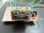
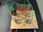
I have designed and built a load resonant full bridge inverter that operates at 85kHz. The inverter is to be used in multi-kilowatt inductive power transfer (Please see attached pictures and video links below for a sample of the set-up). I’m presently in the process of characterizing the inverter’s switching losses and by extension its efficiency. Accordingly, all I have at my disposal to get the job done is a Tektronix TPS2024 isolated channel scope that is outfitted with the TPS2PWR1 power analysis application software. For my probes I have the following: P5122 high voltage probe and an A622 current clamp.
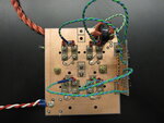
My question is this: the instruction manual for the power analysis application calls for the placement of the current probe at the collector/drain of the switching device (see instruction manual quotation below), however, my present PCB layout (indeed any practical layout for that matter), does not permit for the placement of the large A622 current clamp at the collector/drain of the semiconductor.
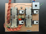
That being said, I was thinking that I could probe the output of the inverter instead because I have easy access to it through the Litz conductor that interfaces my resonant load and the inverter bridge. I wanted to confirm whether this approach would be correct. Thanks in advance for any assistance you may be able to provide.
Regards,
Bryan
TPS2PWR1 Switching Loss Set-up Instructions:
“Place an isolated, floating voltage probe, across the devices collector and emitter. Place a current probe, to measure the collector current.”
“Connect the current probe in the collector leg. Alternatively, you may connect the current probe in the emitter leg. However, the emitter current includes the gate drive current, which may be significant.”
VIDEO LINKS:
https://www.youtube.com/watch?v=O7ngvz1OmGk
https://www.youtube.com/watch?v=R4ifaGinIGE
I have designed and built a load resonant full bridge inverter that operates at 85kHz. The inverter is to be used in multi-kilowatt inductive power transfer (Please see attached pictures and video links below for a sample of the set-up). I’m presently in the process of characterizing the inverter’s switching losses and by extension its efficiency. Accordingly, all I have at my disposal to get the job done is a Tektronix TPS2024 isolated channel scope that is outfitted with the TPS2PWR1 power analysis application software. For my probes I have the following: P5122 high voltage probe and an A622 current clamp.
My question is this: the instruction manual for the power analysis application calls for the placement of the current probe at the collector/drain of the switching device (see instruction manual quotation below), however, my present PCB layout (indeed any practical layout for that matter), does not permit for the placement of the large A622 current clamp at the collector/drain of the semiconductor.
That being said, I was thinking that I could probe the output of the inverter instead because I have easy access to it through the Litz conductor that interfaces my resonant load and the inverter bridge. I wanted to confirm whether this approach would be correct. Thanks in advance for any assistance you may be able to provide.
Regards,
Bryan
TPS2PWR1 Switching Loss Set-up Instructions:
“Place an isolated, floating voltage probe, across the devices collector and emitter. Place a current probe, to measure the collector current.”
“Connect the current probe in the collector leg. Alternatively, you may connect the current probe in the emitter leg. However, the emitter current includes the gate drive current, which may be significant.”
VIDEO LINKS:
https://www.youtube.com/watch?v=O7ngvz1OmGk
https://www.youtube.com/watch?v=R4ifaGinIGE