faisal78
Member level 3

- Joined
- Aug 27, 2004
- Messages
- 62
- Helped
- 0
- Reputation
- 0
- Reaction score
- 0
- Trophy points
- 1,286
- Activity points
- 592
Hi
In reference to a typical MCU GPIO model today, it seems that many if not all manufacturers would implement a diode to VCC and another diode to VSS on all GPIO inputs.
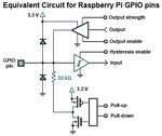
See image for reference example on Rasberry Pi.

1. It seems logical that these diode were implemented for ESD protection reasons. However, in a ESD event, the lower diode would be in conduction to from the input pin to VSS.
I don't see the reason for the diode on the upper VDD side?
Can somebody shed some light?
2. How would a signal overshoot and undershoot behave in this GPIO model. I don't see how a short few ns of undershoot of <-0.7v would cause any damage to the IO.
Please help.
In reference to a typical MCU GPIO model today, it seems that many if not all manufacturers would implement a diode to VCC and another diode to VSS on all GPIO inputs.
See image for reference example on Rasberry Pi.

1. It seems logical that these diode were implemented for ESD protection reasons. However, in a ESD event, the lower diode would be in conduction to from the input pin to VSS.
I don't see the reason for the diode on the upper VDD side?
Can somebody shed some light?
2. How would a signal overshoot and undershoot behave in this GPIO model. I don't see how a short few ns of undershoot of <-0.7v would cause any damage to the IO.
Please help.
