Continue to Site

Welcome to EDAboard.com

Welcome to our site! EDAboard.com is an international Electronics Discussion Forum focused on EDA software, circuits, schematics, books, theory, papers, asic, pld, 8051, DSP, Network, RF, Analog Design, PCB, Service Manuals... and a whole lot more! To participate you need to register. Registration is free. Click here to register now.

MAX485 signal mystery

Status
Not open for further replies.

earckens

Junior Member level 2
Joined
Aug 25, 2016
Messages
21
Helped
0
Reputation
0
Reaction score
0
Trophy points
1
Location
Ghent
Activity points
151
EDIT: I am not sure this was posted in the correct subcategory?

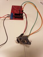
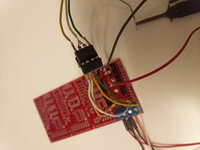
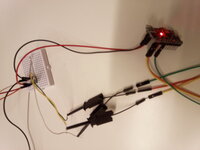
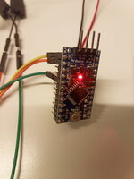
A simple circuit with a MAX485 (attachement 1) works perfectly when used in a breadboard setup. However, as soon as the test is transferred to a fabricated pcb this circuit does not work.

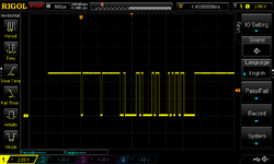
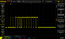
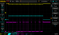
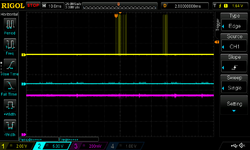
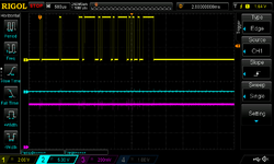
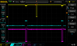
1. The RS485 link receives valid data which is correctly parsed in the breadboard dcircuit. The RX line receives data (see attachment 3: scope printout), the DE line is properly pulsed when TX wants to send its reply. The master acknowledges receipt.

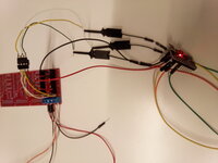
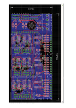
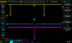
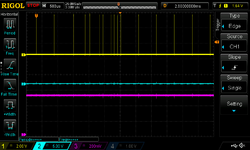
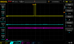
2. However, when using the PCB design (attachment 2), RX is still properly received at slave controller level (stil same image as attachment 3) but DE does not respond: level stays low, ie no intention to transmit.

Same software, same controller.
When reverting back to the breadboard setup all functions as should be.

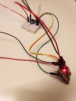
When in breadboard modus I connected DE from the breadboard setup to the PCB (with a MAX485 soldered in place, under power: all still ok (to make sure there are no PCB issues with the DE line).

When removing the soldered MAX485 from the pcb for testing: it functions well, all ok.

I am "end of line" after two days of testing; any help would be very greatly appreciated!

Code:
/* http://www.utrainia.com/65-arduinocmri-and-rs485
/* Arduino CMRI and RS485
*/

#include <Auto485.h>
#include <CMRI.h>

#define CMRI_ADDR 0

#define    DE_PIN 2
#define   LED_PIN 13

Auto485 bus(DE_PIN); // Arduino pin 2 -> MAX485 DE and RE pins
CMRI cmri(CMRI_ADDR, 24, 48, bus); // defaults to a SMINI with address 0. SMINI = 24 inputs, 48 outputs

void setup() {
  pinMode(LED_PIN, OUTPUT);
  bus.begin(19200);
}

void loop() {
  // 1: main processing node of cmri library
  cmri.process();
 
  // 2: update output. Reads bit 0 of T packet and sets the LED to this
  digitalWrite(LED_PIN, cmri.get_bit(0));
 
  // 3: update input. Flips a bit back and forth every second
  cmri.set_bit(0, (millis() / 1000) % 2 == 0);
}
 

Attachments

  • MAX485 pcb.pdf
    67.1 KB · Views: 171
  • MAX485 circuit.pdf
    181.8 KB · Views: 177
  • DS1Z_QuickPrint1.png
    DS1Z_QuickPrint1.png
    39.3 KB · Views: 132
Last edited:

Hi,

You say:
* on breadboard it is working
* on PCB it's not working

But you
* neither show what you did on breadboard,
* nor what you did on PCB.

So how can we find out what's the difference?

Klaus
 

Hi,

You say:
* on breadboard it is working
* on PCB it's not working

But you
* neither show what you did on breadboard,
* nor what you did on PCB.

So how can we find out what's the difference?

Klaus
Hi KlausST,

on the breadboard I used exactly the same wiring as on the PCB:

A & B incoming signal connected to pins 6 & 7.
/RE and DE connected together and connected to controller pin 2
RO from MAX485 to RX of controller
DI from MAX485 to TX of controller.

The RX wire is orange, TX yellow, DE (pin 2) is green.
Data cable is twisted white/orange.

On the RX wire there always is data shown as in screenprint from scope in my initial post.
 

Attachments

  • IMG_20220115_064354.jpg
    IMG_20220115_064354.jpg
    1.6 MB · Views: 118
  • IMG_20220115_070029.jpg
    IMG_20220115_070029.jpg
    1.6 MB · Views: 117

Hi,

It seems to be an EAGLE layout.
Did you run the DRC? Some signals seem to be "more than close" to each other.

There are a lot of issues makinkg validation difficult: Non standard symbols, no pin numbering.
The trace routing is from from good .. but could be improved witin a couple of minutes.
GND is cut into pieces (as far as I can imagine) and thus can´t act as a GND plane.

What happend with C9/C7 and C8/C6? (Why in connected parallel and why 180° rotated?)

please use EAGLE commands:
* dis none top bot via pad tpla
* rat
-> then upload the screenshot as .PNG (area a bit wider than in your .PDF)

Klaus

Added:
Sadly in your photos we can´t see which wire goes to which pin (But this is important if you want us to give advice). They don´t seem to be wired equally.
 
Last edited:

Basic information missing. What's the peer in your test? How are the communication roles?

Error description suggests that your device has slave role, is receiving some RX data, but not recognizing it. Besides specific circumstances, e.g. comparision with breadboard behaviour, there's a basic way to analyze the received data, check if it arrives correctly at the microcontroller receive routine and why it's not recgnized as valid request.

1. The RX signal can be checked for valid serial frame characteristics. You can identify the baud rate and even decode messages in the oscilloscope waveform. Ideally your oscilloscope can decode UART protocols and display the data bytes. RX line should have high idle state, but we don't know where the captured data stream actually starts. There might a problem of reversed polarity or missing RS485 pull-up/-down resistors.

2. Use Arduino debugging methods to check how the incoming data is seen by the UART.
 

Hi,

It seems to be an EAGLE layout.
Did you run the DRC? Some signals seem to be "more than close" to each other.

There are a lot of issues makinkg validation difficult: Non standard symbols, no pin numbering.
The trace routing is from from good .. but could be improved witin a couple of minutes.
GND is cut into pieces (as far as I can imagine) and thus can´t act as a GND plane.

What happend with C9/C7 and C8/C6? (Why in connected parallel and why 180° rotated?)

please use EAGLE commands:
* dis none top bot via pad tpla
* rat
-> then upload the screenshot as .PNG (area a bit wider than in your .PDF)

Klaus

Added:
Sadly in your photos we can´t see which wire goes to which pin (But this is important if you want us to give advice). They don´t seem to be wired equally.
The DRC is set up per manufacturer requirements. The ground plane is a polygon on the back, connected where needed, no missing connections.

Basically this is a ridiculously simple circuit: RS485 A & B going to pins 6 & 7.
RO from MAX485 to RX of controller.
DI from MAX485 to TX of controller.
DE and /RE shorted and to pin 2 of controller.
 

Attachments

  • Arduino-CMRI_SMD_v4.pdf
    78.9 KB · Views: 131

Basic information missing. What's the peer in your test? How are the communication roles?

Error description suggests that your device has slave role, is receiving some RX data, but not recognizing it. Besides specific circumstances, e.g. comparision with breadboard behaviour, there's a basic way to analyze the received data, check if it arrives correctly at the microcontroller receive routine and why it's not recgnized as valid request.

1. The RX signal can be checked for valid serial frame characteristics. You can identify the baud rate and even decode messages in the oscilloscope waveform. Ideally your oscilloscope can decode UART protocols and display the data bytes. RX line should have high idle state, but we don't know where the captured data stream actually starts. There might a problem of reversed polarity or missing RS485 pull-up/-down resistors.

2. Use Arduino debugging methods to check how the incoming data is seen by the UART.
This device acts as a slave.

Yes data arrives properly at the controller (scope screenshot in first post).
Baud rates for master and slave are synchronised (19200), comms work in breadboard "mode".
RX is idle low.
MAX485 states no resistors required in RX and TX lines.
Incoming line might need 120R for longer distances but here we talk 1 foot.

Reversed polarity etc.. would be the same issue in breadboard mode. Where it works ok.

"Breadboard mode": exactly copy/past the same wiring and the same component as on PCB.

At the moment I have soldered wires to the SOP8 PCB pads and connected a DIP8 socket for a DIP MAX485. So I can at a whim interchange the same chip and controller wiring from PCB to breadboard.

I isolated RX, TX and DE wires from the PCB when in PCB mode, still the same issue.

I isolated the A & B incoming wires from the PCB when in PCB mode, still the same issue.

When then back to breadboard with the same components, it works.

When back to PCB with only incoming A & B via PCB: doesn't work.

When adding 120R between A & B: still not working.

And all the while the incoming RX data to the controller is nice, clean. But on the PCB no reaction from pin 2 to start transmission.
 

Hi,

Sadly I was not clear enough with
* the EAGLE command
* the .PNG
* the photos

Klaus
--- Updated ---


quite unusual

Klaus
Why?


Per page 10 of the datasheet it shows "RO normally low" or "RO normally high" (RO goes to RX).
 

Attachments

  • MAX485 transceiver RS485.pdf
    636.3 KB · Views: 132

Hi,

You didn´t perform the EAGLE commands as given
You didn´t upload the PNG, but a PDF
You don´t show photos where we can verify the wiring.

*****
On UART signals Rx as well as Tx are idle HIGH.
I see that the MAX458 has a grey zone between -200mV and +200mV for (A-B).
So this might cause the "not idle HIGH".
Better use some 700 Ohms biasing resistors to pull A with to +5V and B to GND.

Also when RE=1 then RO = HIGH-Z, thus the state is undefined. Better use a pull up to get known and valid levels

Klaus
 

Hi,


You didn´t perform the EAGLE commands as given
You didn´t upload the PNG, but a PDF
You don´t show photos where we can verify the wiring.

*****
On UART signals Rx as well as Tx are idle HIGH.
I see that the MAX458 has a grey zone between -200mV and +200mV for (A-B).
So this might cause the "not idle HIGH".
Better use some 700 Ohms biasing resistors to pull A with to +5V and B to GND.

Also when RE=1 then RO = HIGH-Z, thus the state is undefined. Better use a pull up to get known and valid levels

Klaus
Sorry to read your comments:
1. I do not understand what you mean by "Eagle comments". But the board is finished to the requirements of the fab.
2. A pdf was uploaded because that is what I got from Eagle
3. Photos to verify wiring: if I confirm that my wiring is checked and double checked then I am satisfied there is no issue with my connections/wiring. I trust you do your best to try and find with me the issue at hand here. I hope you trust me when I say that the wiring is not the issue.

The state of RX and TX are determined by the software library in the controller when in high Z.
Adding a terminator resistor does not solve the problem, nor do the biasing resistors: trial performed just now.

Tomorrow I will connect a logic analyser and compare the data on RX when in the breadboard and when on the PCB.
 

Hi
I do not understand what you mean by "Eagle comments"
--> command:
just copy and paste this: [dis none top bot via pad tpla] to the EAGLE command line and press the ENTER button. ;-)
.. undo with [dis last]

that is what I got from Eagle
Every OS lets you do a screenshot.
additionally EAGLE lets you export an image

I confirm that my wiring is checked
Yes, I´ve read this very often in the forum .....

Nothing against you. It´s the human brain that "sometimes just sees what it expects to see". Look at this:
..Aoccdrnig to a rscheearch at Cmabrigde Uinervtisy, it deosn't mttaer in waht oredr the ltteers in a wrod are...

Especially when you did the writing/paining/wiring/soldering on your own.
A second "pair of eyes" does not have the same expectation than you have. Thus it will see much more mistakes.

Klaus
 

Ah ok, screenshot of .brd: see attached.
Also pictures of setup: both breadboard, and PCB, with exactly same controller and MAX485.
Also scope printscreen or RX both for breadboard (2) and PCB (3).
 

Attachments

  • IMG_20220115_193614.jpg
    IMG_20220115_193614.jpg
    147 KB · Views: 112
  • DS1Z_QuickPrint3.png
    DS1Z_QuickPrint3.png
    38.9 KB · Views: 112
  • DS1Z_QuickPrint2.png
    DS1Z_QuickPrint2.png
    42.5 KB · Views: 114
  • IMG_20220115_193625.jpg
    IMG_20220115_193625.jpg
    147.3 KB · Views: 112
  • IMG_20220115_193217.jpg
    IMG_20220115_193217.jpg
    128 KB · Views: 105
  • IMG_20220115_193153.jpg
    IMG_20220115_193153.jpg
    133.3 KB · Views: 112
  • IMG_20220115_193115.jpg
    IMG_20220115_193115.jpg
    295.4 KB · Views: 109
  • Document2.png
    Document2.png
    2.7 MB · Views: 117

I would consider it a miracle if it worked at all with such long wiring and no decoupling capacitor, you were lucky!

Can you post a picture of the scope trace with RX, TX and the direction control signals on screen at the same time so we can see the relative timing between them.

Brian.
 

Hi,
a comment by Klaus a few posts higher about the high default state of the TX and RX lines, and my yesterdays post where I noticed that default on the working breadboard is high, but not so on the PCB made me look at the polarity of A & B.
Coincidentaly on the breadboard A & B always were correctly inserted, however not so on the PCB.
When inserted swapped on the breadboard it stopped working.

Attached are scope screenshots of breadboard and PCB behaviour. Ch1 (yellow)= RX, Ch2 (blue)= DE and /RE, Ch3 (pink)= TX.
1 & 2: breadboard
3 & 4: PCB with correct A & B connections
5 & 6: PCB with A & B swapped.

What is strange is that:
1. default RX and TX on PCB never goes to high (pics 3 & 4)
2. when A & B are inserted straight on the pcb, just spikes are placed on RX, and when A & B are swapped there are "intelligible" pulses (pics 5 & 6)
--- Updated ---

I would consider it a miracle if it worked at all with such long wiring and no decoupling capacitor, you were lucky!

Can you post a picture of the scope trace with RX, TX and the direction control signals on screen at the same time so we can see the relative timing between them.

Brian.
Hi Brian,
where would you like to see the decoupling capacitors?
Erik
 

Attachments

  • DS1Z_QuickPrint9.png
    DS1Z_QuickPrint9.png
    49.4 KB · Views: 117
  • DS1Z_QuickPrint10.png
    DS1Z_QuickPrint10.png
    39.1 KB · Views: 110
  • DS1Z_QuickPrint11.png
    DS1Z_QuickPrint11.png
    36.2 KB · Views: 105
  • DS1Z_QuickPrint12.png
    DS1Z_QuickPrint12.png
    39.7 KB · Views: 101
  • DS1Z_QuickPrint13.png
    DS1Z_QuickPrint13.png
    34.5 KB · Views: 105
  • DS1Z_QuickPrint14.png
    DS1Z_QuickPrint14.png
    43.6 KB · Views: 102
Last edited:

Decoupling capacitors should be between ground and supply pins of the MCU and the MAX485, as near to the IC as possible. This will be the cause of most of the overshoot on level transitions.

Although the waveform shapes look fine, trace 3 has a 200mV/division height so it only reaches about 0.5V logic '1' level, this is too low to be recognized by 5V or 3.3V logic families.

Brian.
 

Hi,

Is all this 5V supplied or 3.3V supplied? What signal levels?
Does the microcontroller module contain a voltage regulator?

Decoupling capacitors:
Usually I place a ceramics 100nF capacitor very close (max 5mm) at every supply pin of every IC with a via to GND plane.
Only rarely I reduce this capacitor count. It's not uncommon that I have more than 50 of those capacitors on a euro size PCB.
Additionally you should ad a common bulk capacitor. It's location is not that important.

When I'm doing a PCB layout... I place the IC, then I place the decoupling capacitors next to the VCC pin. Short trace to IC, short traces to vias to GND.
Whenever I move the IC I also move the capacitor, vias and traces as a group.

Current (here HF) follows a loop. Check the loop according length and enclosed area:
* capacitor_GND - capacitor_VCC - IC_VCC - IC_GND - GND_plane - capacitor_GND.
Mind: the way back from IC_GND to capacitor_GND is equally important, thus a split in the GND plane kills the performance.
I try to get loop length of less than 15mm and area below 10mm^2. This is not a strict requirement, but this is just my standard procedure. In detail one can differ about possible IC speed (not the used signal frequency! If you run a 100MHz Opamp just with 10kHz of signal freqyency you still have to treat it as 100MHz path. In your case: don't calculate with the used baud rate, but with the frequency component according MAX485's voltage rise rate)

********
Back to your initial problem:
* Please check for soldering problems at each IC leg.
* install biasing resistors to get out of the zone of non valid voltage level.

Klaus
 

@brian: trace 3 (pink) effectively is a 2V/div signal, but the scope had inadvertently been set at x10 instead of x1 for this channel as that is the actual probe setting.

I think the issue is solved.

A and B polarity do matter here: I had disregarded this requirement.

Attached: scope screen from PCB.

Thank you all for your greatly appreciated contributions!

Klaus for your hinting at default state for TX and RX, Brian for your request for scope screenshots.
 

Attachments

  • DS1Z_QuickPrint15.png
    DS1Z_QuickPrint15.png
    39.2 KB · Views: 93

I'm glad it is resolved. A and B are equal but opposite voltage levels so if swapped, the traces will still look correct but the UARTs at each end will not be able to frame the bytes correctly.

Brian.
 

I'm glad it is resolved. A and B are equal but opposite voltage levels so if swapped, the traces will still look correct but the UARTs at each end will not be able to frame the bytes correctly.

Brian.
Is there a way to correct this in software? The controller I use (AtMega328 in "pro mini" version) does not have a UART chip, TX and RX are directly read by the controller.

EDIT: By "correct" I mean: allow for polarity inversion.

Code:
/* http://www.utrainia.com/65-arduinocmri-and-rs485
/* Arduino CMRI and RS485
*/

#include <Auto485.h>
#include <CMRI.h>

#define CMRI_ADDR 0

#define    DE_PIN 2
#define   LED_PIN 13

Auto485 bus(DE_PIN); // Arduino pin 2 -> MAX485 DE and RE pins
CMRI cmri(CMRI_ADDR, 24, 48, bus); // defaults to a SMINI with address 0. SMINI = 24 inputs, 48 outputs

void setup() {
  pinMode(LED_PIN, OUTPUT);
  bus.begin(19200);
}

void loop() {
  // 1: main processing node of cmri library
  cmri.process();
 
  // 2: update output. Reads bit 0 of T packet and sets the LED to this
  digitalWrite(LED_PIN, cmri.get_bit(0));
 
  // 3: update input. Flips a bit back and forth every second
  cmri.set_bit(0, (millis() / 1000) % 2 == 0);
}
 

Attachments

  • Arduino Pro Mini Schematic.pdf
    45.7 KB · Views: 118
Last edited:

Status
Not open for further replies.

Similar threads

Part and Inventory Search

Welcome to EDABoard.com

Sponsor

Back
Top