Continue to Site

Welcome to EDAboard.com

Welcome to our site! EDAboard.com is an international Electronics Discussion Forum focused on EDA software, circuits, schematics, books, theory, papers, asic, pld, 8051, DSP, Network, RF, Analog Design, PCB, Service Manuals... and a whole lot more! To participate you need to register. Registration is free. Click here to register now.

LM5116 buck converter problem - not working

Status
Not open for further replies.

krishnakumar.r93

Member level 2
Joined
Jan 28, 2015
Messages
48
Helped
1
Reputation
2
Reaction score
1
Trophy points
8
Activity points
388
Hi guys

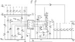
I tried a buck converter using LM5116 with reference to the schematic in section 8.2 of the LM5116 datasheet , which is designed for an output of 5VDC / 7A.

My problem is that, inspite of having used the exact values of the components mentioned in the schematic, I don't get the specified output. Instead I get Vout = Vin, where in i changed my Vin from 10VDC to 50VDC. Somebody please help me ASAP.

Below I've attached the same schematic for reference.
 

Attachments

  • Schematic.jpg
    Schematic.jpg
    467.5 KB · Views: 375
  • lm5116.pdf
    1.5 MB · Views: 116

Hi,

please give us YOUR schematic.
And please post a photo form your circuit.

***
I know you use the same parts as in the LM datasheet.
But I don´t like the MOSFET selection. It is rated with ABSOLUTE MAXIMUM of 60V. But the application say input voltage up to 60V. So any little spike at the MOSFET will run it out of specification.

With a good low impedance pcb layout (almost free of spikes) I recommend at least 20% headroom (--> 75V). With a standard layout even 100% may not be sufficient.

Klaus
 

Hi,
please give us YOUR schematic.

Klaus

I've attached MY schematic for ur reference.


Hi,
But I don´t like the MOSFET selection.
Klaus

I've tried using the Si7810DP MOSFET as well, which is 100V max, but there is no change in the output, ie., Vout=Vin.
 

Attachments

  • schematic.pdf
    79.7 KB · Views: 151

Hi,

in your schematic of post#3 there is a GND connection missing. PGND to AGND.

Klaus
 

Hi,

in your schematic of post#3 there is a GND connection missing. PGND to AGND.

Klaus

The AGND and PGND are connected under the LM5116. I've attached the image for reference, showing the connection between AGND and PGND (pin 6 and pin 14)


But there is no connectivity between the i/p ground and the o/p ground.
I also need a suggestion, shall i directly connect both the ground by means of a wire?
 

Attachments

  • PGND- AGND connected.png
    PGND- AGND connected.png
    231.7 KB · Views: 162

Hi,

for sure you need to connect ALL GNDs.
(In the datasheet schematic you see all GNDs are connected via the GND symbols)

It seems you don´t have a solid GND plane. But it is very important for switch mode power supplies to have reliable, stable, low impedance GND connections.


Klaus
 
Hi,

for sure you need to connect ALL GNDs.
Klaus

Interconnecting both the AGND and PGND gives the output, but not 5V. Instead i get stable 19V o/p when my input is 45v to 60v.

Made calculations for the Output Vout=12V. Changed the component values. What are the component values that i need to change for getting a fixed 12v o/p for the input range 17V to 80VDC?
 

Hi,

The datasheet is your friend:

********
8.2.2.10 Output Voltage Divider
RFB1 and RFB2 set the output voltage level, the ratio of these resistors is calculated from:
R_FB2/R_FB1 = (V_OUT / 1.215V) - 1 (24)
RFB1 is typically 1.21 kΩ for a divider current of 1 mA. The divider current can be reduced to 100 μA with
RFB1=12.1 kΩ. For the 5V output design example used here, RFB1 = 1.21 kΩ and RFB2 = 3.74 kΩ.
********

Klaus

Is only the RFB1 and RFB2 enough? I had changed the value of L, Rt and Cramp.
 

Hi,

R_FB1 and R_FB2 set the output voltage.

All other changes are for proper operation of the regulator.

(Imagine R_FB1 and R_FB2 act like a steering wheel of a car. But to keep track you additionally need to adjust your car speed to the road surface.)
-->
* A percentual change in R_FBx results in an percentual change in V_OUT
But:
* A percentual change in L will not change output voltage
* A percentual change in Rt will not change output voltage
* A percentual change in CRamp will not change output voltage


Klaus

I have the following component values:

L = 22uH
Rt = 12.4k
Cramp = 276pF
Rfb1 = 1.21k
Rfb2 = 10k

I get 12v o/p only when i/p is 60v - 80v without load at o/p.
When i connect a load, my o/p doesnt even cross 6v even at 100v i/p. Instead the o/p voltage varies from 4.8v to 6v for input ranging from 8v-100v.
 

Hi,

I'm guessing
* PCB layout problem (we can't review, because you didn't give this picture)
* part selection. Especially all Ls, Cs and Ds. A single value (like 22uH) is not enough. We need the datasheets to be able to review them.

Klaus
 

Hi,

I'm guessing
* PCB layout problem (we can't review, because you didn't give this picture)
* part selection. Especially all Ls, Cs and Ds. A single value (like 22uH) is not enough. We need the datasheets to be able to review them.

Klaus

Do you need the picture of the PCB or the layout design.? I've attached a pic of the layout design.
 

Attachments

  • PCB layout.png
    PCB layout.png
    160.6 KB · Views: 103
Last edited:

Hi,

No GND plane?... those thin wires for low impedance connections?...No wonder i doesn´t work.

Didn´t you read the datasheet? ... and the layout guidelines?

Klaus
 

Hi,

No GND plane?... those thin wires for low impedance connections?...No wonder i doesn´t work.

Didn´t you read the datasheet? ... and the layout guidelines?

Klaus

I read the datasheet and followed it except for the ground plane on the PCB.

How thick should my wires be? (I've used 15thous)
How do i calculate the impedance of my connections and how does it affect the performance?

- - - Updated - - -

Actually, I kindof got the output by changing the Rfb1 and Rfb2 as stated in my post#11.
I changed the inductor value from 22uH to 10uH and Cramp = 330pF, the remaining components same. (Rt = 12.4k, Rfb1 = 1.21k, Rfb2 = 10k).
The output of this was, 3.8-5v without load with i/p varying from 10v to 80v. With load, the o/p was 3.8v for i/p varying from 10v to 80v.

After this attempt, whatever values of Rfb1 and Rfb2 i use, i get only 3.8v o/p with load and without load.
I even tried undoing the component value changes and still no change in the output.
 

Hi,

I read the datasheet and followed it
When you look at the layout example of the datasheet you see that there are actually no "wires" but completely filled areas.
And only some mm short.

Your wires are ten times longer but only 1/10 wide. This makes it 100 times worse.

You can play with many part values, but your layout is not suitabe for switch mode supplies. It´s a waste of time.
Don´t expect to get it work...Sorry, I can´t give you hope.

You really need to keep on the guidelines. Design a new PCB.

Klaus

- - - Updated - - -

Added:

And please post your PCB layout BEFORE you produce the PCB.
We will help you to get good results.

Also still missing: a detailed description of your parts. As said 22uH is not enough information to validate an inductance.

Klaus
 
And please post your PCB layout BEFORE you produce the PCB.
We will help you to get good results.

Also still missing: a detailed description of your parts. As said 22uH is not enough information to validate an inductance.

Klaus
Added:
Yeah, thanks. I'll make sure to consults before outsourcing the PCB for fabrication.
 

Hi,


When you look at the layout example of the datasheet you see that there are actually no "wires" but completely filled areas.
And only some mm short.

You really need to keep on the guidelines. Design a new PCB.
Klaus

Should i design a double-sided board with ground plane on both sides, or is it enough if i just make a single-sided board with ground plane on one side?
 

Hi,

the GND plane improves signal quality, but it also helps to distribute the heat.

--> single sided GND plane is sufficient. Via count improves low impedance and improves thermal conductivity.

Klaus
 

Hi,

the GND plane improves signal quality, but it also helps to distribute the heat.

--> single sided GND plane is sufficient. Via count improves low impedance and improves thermal conductivity.

Klaus

As per your suggestion, I have changed the PCB design with a ground plane copper fill. Please check the design and let me know if it is enough.
 

Attachments

  • PCB layout.png
    PCB layout.png
    57.9 KB · Views: 172

Status
Not open for further replies.

Similar threads

Part and Inventory Search

Welcome to EDABoard.com

Sponsor

Back
Top