Continue to Site

Welcome to EDAboard.com

Welcome to our site! EDAboard.com is an international Electronics Discussion Forum focused on EDA software, circuits, schematics, books, theory, papers, asic, pld, 8051, DSP, Network, RF, Analog Design, PCB, Service Manuals... and a whole lot more! To participate you need to register. Registration is free. Click here to register now.

LM317 High Current Regulator

Status
Not open for further replies.

boylesg

Advanced Member level 4
Joined
Jul 15, 2012
Messages
1,023
Helped
5
Reputation
10
Reaction score
6
Trophy points
1,318
Location
Epping, Victoria, Australia
Activity points
11,697
Could some one please explain how you calculate the values of R3 and R6 in this circuit the following circuit.

I had a go at plugging the appropriate values into a Excel spread sheet calculator I have made for transistors in switching mode.

So I chose the maximum output current for my Q2 at 5A and then calculated the required base current using my spreadsheet. That gave me a required base current of 50mA which seems about right according to 2SD2045 datasheet.

Then I used this as the collector current for my BC327 and tried to calculate the required base current and base resistor value using the same spread sheet. That's where I got the erroneous value for the base resistor of BC327.

I came up with value of 100k, or there abouts, for R3 and naturally Q1 and Q2 never switch on in the simulator when I reduce the load resistance to a very low value.

The formulas in my spread sheet were taken from an NPN example I found. So I am presuming that the formulas used for calculating the resistors etc for a PNP transistor a different to those used for NPN transistors.

The values for R3 and R6 in the simulator are based on the values specified in the LM317 datasheet for a high current voltage regulator.

Q2 is an approximation for 2SD2045 that I will actually use in the real circuit.
 

Actually after a few days of digging I found this page: https://www.dnatechindia.com/Tutorial/Transistors/Bipolar-Transistor.html

The common collector amplifier down the page is identical to the arrangement of Q1, R3 and R5.

So Q1 is configured as a common collector amplifier which makes sense because you want to amplify the small current flowing from its base, as a result of the small voltage drop across R2, to a current large enough to turn on Q2.

So if I plug some values for BC327 into my common collector amplifier calculation table, I should come up with similar resistor values once I figure out what amplifier gain value they have used in the datasheet for LM317.
 

Could some one please explain how you calculate the values of R3 and R6 in this circuit........
R6 determines how much current must flow through Q1 before Q2 switches on. 560 Ohms is fine. It sets that current to about 2mA.

R3 isn't important, it just protects Q1's base if something goes badly wrong in the rest of the circuit. You can leave it out. If you want to use it, 1K or 2K should be OK.

So Q1 is configured as a common collector amplifier......
Q1 is common emitter.
Q2 is common collector.
 

Q1 is common emitter.
Q2 is common collector.

Oh!

For some reason I find it very confusing figuring out what sort of amplifier transistors are arranged in when they are not arranged in a really 'traditional' way (if I can call it that) as in the TransistorAmp software I have been using.

The fact that Q1 is a PNP where as all the amplifiers in TransistorAmp are based on NPNs no doubt adds a bit to my confusion.

R6 determines how much current must flow through Q1 before Q2 switches on. 560 Ohms is fine. It sets that current to about 2mA.
So I take it then that it is just a straight V=IR thing?

R3 isn't important, it just protects Q1's base if something goes badly wrong in the rest of the circuit. You can leave it out. If you want to use it, 1K or 2K should be OK.

Any particular reason why would you personally choose these values rather than the 5K specified in the datasheet?
 

For some reason I find it very confusing figuring out what sort of amplifier transistors are arranged in when they are not arranged in a really 'traditional' way
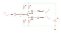
Easy guide:
  • Common emitter: Input to base, output from collector
  • Common collector: Input to base, output from emitter
  • Common base: Input to emitter, output from collector
Sometimes you see a combination. For example; in the circuit below the transistor is acting as a common emitter and a common collector at the same time.


Any particular reason why would you personally choose these values rather than the 5K specified in the datasheet?
Not really. I hadn't seen it in a datasheet, but I found it now in the National datasheet. 5K is OK too. If you make the resistor too big though, it will start significantly reducing the maximum output voltage. Each volt across that resistor is one less volt you can have at the output.

BTW, The value of R2 looks very low. The datasheet suggests 22R, but you're using 3.9R. That means the LM317 has to carry a lot of current before the transistors turn on.
 

In the simulator, if I make R3 10K and leave R6 alone then it limits the output current of Q2 to about 5A with about 1R load.

So that is a good thing given that I am using 2SD2045 darlington with a 6A max EC current.

From the TransistorAmp software the ratio between R1 and R3 partly determines the voltage gain of CE amplifier.

But it is still a bit hard to follow the pattern with the CE amplifier in this circuit because it lacks R2 and R4 that the TransistorAmp CE amplifier has, where R4 also determines the voltage gain in combination with R1 and R3.
 

Any suggestions on how I can add some LEDs into this circuit to indicate separately when the LM317 is supplying voltage and when Q2 is supplying a current boost of say 100mA or more.

I have tried a few spots, with both in the real circuit and the simulator, but each time it seems to either upset the operation of the LM317 circuitry or the turn on of Q2 or else the LED lights regardless of whether Q2 is on or off.
 

Status
Not open for further replies.

Part and Inventory Search

Welcome to EDABoard.com

Sponsor

Back
Top