tomjal
Newbie
Hi,
Before I start, I need you guys to know that this is new and the first time for me to do this kind of thing, but I still need to do this anyway.
Here's what I have:
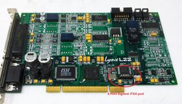
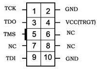
2x Lynx L22 PCI Audio Interface (Picture below with the 6 JTAG pinouts): 1 with bad firmware, 1 with working firmware)
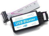
Altera USB Blaster 10 pins JTAG (Picture below): For the connector from board to PC
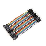
Some dupont wires: to connect the 10pins to 6 pins JTAG
UrJTAG software: for the firmware extraction and insertion.
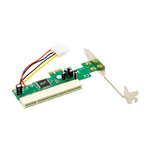
PSU with molex and PCIe to PCI adapter (Picture below): to power the board
Again, please correct me if I'm wrong, I'm so new.
Here's the steps I'm gonna make:
1. I'm gonna power up the donor board directly using my PCI adapter and molex to the adapter.
2. connect my USB Blaster 10 pins (Pinouts picture below) to the PCI 6 pins(Pinouts picture below). Also I'll put the extra pin out explanation below.
3. Connect USB Blaster to PC and start UrJTAG
5. Follow firmware extraction from this article https://embeddedbits.org/2020-02-20-extracting-firmware-from-devices-using-jtag/
6. Once I get the ROM, do the same thing to the bad PCI card but with insertion of firmware from the previous card.
Pinouts from 10 to 6 pins:
I think that's all for now. Thank you everybody!
[moderator action: added CODE tags to improve visibility of connections]
Before I start, I need you guys to know that this is new and the first time for me to do this kind of thing, but I still need to do this anyway.
Here's what I have:
2x Lynx L22 PCI Audio Interface (Picture below with the 6 JTAG pinouts): 1 with bad firmware, 1 with working firmware)
Altera USB Blaster 10 pins JTAG (Picture below): For the connector from board to PC
Some dupont wires: to connect the 10pins to 6 pins JTAG
UrJTAG software: for the firmware extraction and insertion.
PSU with molex and PCIe to PCI adapter (Picture below): to power the board
Again, please correct me if I'm wrong, I'm so new.
Here's the steps I'm gonna make:
1. I'm gonna power up the donor board directly using my PCI adapter and molex to the adapter.
2. connect my USB Blaster 10 pins (Pinouts picture below) to the PCI 6 pins(Pinouts picture below). Also I'll put the extra pin out explanation below.
3. Connect USB Blaster to PC and start UrJTAG
5. Follow firmware extraction from this article https://embeddedbits.org/2020-02-20-extracting-firmware-from-devices-using-jtag/
6. Once I get the ROM, do the same thing to the bad PCI card but with insertion of firmware from the previous card.
Pinouts from 10 to 6 pins:
Code:
USB BLASTER          >           JTAG 6 PINS
TCK   GND                           TMS
TDO   VCC(TRGT)                     TDI
TMS   NC                            TDO
NC    NC                            TCK
TDI   GND                           GND
                                    VIO
Code:
I'm going to connect (obviously)
TMS  >  TMS
TDI  >  TDI
TDO  >  TDO
TCK  >  TCK
GND  >  GND
VIO  >  VCC (Is this one correct or should I just leave it open?)
I think that's all for now. Thank you everybody!
[moderator action: added CODE tags to improve visibility of connections]
Attachments
-
 bcf71373-971a-4843-a175-7fdccad682d4.jpg361.8 KB · Views: 192
 -
 ADP-PX1-PCI-2-800x800.jpg97.9 KB · Views: 197
 -
 download (1).jpg8.1 KB · Views: 191
 -
 80828b4ef4dc27a73b097106b217cf46.jpg104.4 KB · Views: 190
 -
 download (2).jpg5.5 KB · Views: 194
 -
 download (2).jpg5.5 KB · Views: 185
 -
 ove2.png109.8 KB · Views: 203
Last edited by a moderator: