Continue to Site

Welcome to EDAboard.com

Welcome to our site! EDAboard.com is an international Electronics Discussion Forum focused on EDA software, circuits, schematics, books, theory, papers, asic, pld, 8051, DSP, Network, RF, Analog Design, PCB, Service Manuals... and a whole lot more! To participate you need to register. Registration is free. Click here to register now.

is it possible to design a ldo with following specs..???

Status
Not open for further replies.

niya7820

Newbie level 3
Joined
Oct 14, 2014
Messages
4
Helped
0
Reputation
0
Reaction score
0
Trophy points
1
Activity points
28
hello,
is it possible to design LDO using cmos technology with following specs:
vin=2.5v
vou=1.2-1.8v
vref=1.25v
Iomax=upto 1 ampere(i.e around 700mA)

i have to do this for my project work.kindly give your suggestion regarding this specs.as sooon as possible.
software to be used is cadence.

niya
 

Yes it is possible except the output driver is low RdsOn.
-examining your drop, 0.7V min to 1.3Vmax @700mA implies RdsOn is 1 to 2 Ohms and P=0.7V²/1Ω @Vout-max and 1.3V²/2Ω @Vout-min implies RdsOn =<1Ohm with high gain { negative feedback OA } to reduce effective Zout and load regulation error.

Power dissipation loss becomes >0.8W is best done with large N-FET.

If you parallel 22x CMOS (22 OhmESR) 'LVC2 type CMOS or simply N-MOS drivers it might work. or increase N FET area to perform as 1 external MOSFET.

Any of these external N Fets are suitable.


However above is for educational purposes only. why "RE-INVENT the wheel"' when hundreds of solutions exist already.


hello,
is it possible to design LDO using cmos technology with following specs:
vin=2.5v
vou=1.2-1.8v
vref=1.25v
Iomax=upto 1 ampere(i.e around 700mA)

i have to do this for my project work.kindly give your suggestion regarding this specs.as sooon as possible.
software to be used is cadence.

niya
 
thanku sir..
i dont have to use existing specs.and i m trying this design with PMOS.
0.7v drop is normal for ldo design?
can u help me for how to initiate this design.
like how to decide the aspect ratio of mos and which error amplifier shuld i use...
 
Last edited by a moderator:

First review how existing designs are spec'd in my example link and then choose your own specs, from which all designs must begin. Read how they work in the block diagrams.

Good Implementation will always follow good specs. APriori , ipso facto.
 

Yeah you can get PMOS FETs that can handle that much current in CMOS, but I don't know if they will do so with Vgs at only -2.5V. Might actually be easier with a PNP BJT.
 
thank you..!!

how we can choose between different topologies for designing an error amplifier for LDO.
which one will suit my specs ?
1)single differential pair gain stage
2) cs gain stage
3)source follower stage
 

First review how existing designs are spec'd in my example link and then choose your own specs, from which all designs must begin. Read how they work in the block diagrams.

Good Implementation will always follow good specs. APriori , ipso facto.

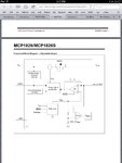
You aren't following good advice. Find what is used now and why from my existing solutions link.... Repeated here.. Scan thru block,diagrams e.g. And learn


image.jpg
 

Status
Not open for further replies.

Similar threads

Part and Inventory Search

Welcome to EDABoard.com

Sponsor

Back
Top