Continue to Site

Welcome to EDAboard.com

Welcome to our site! EDAboard.com is an international Electronics Discussion Forum focused on EDA software, circuits, schematics, books, theory, papers, asic, pld, 8051, DSP, Network, RF, Analog Design, PCB, Service Manuals... and a whole lot more! To participate you need to register. Registration is free. Click here to register now.

IR2110 - High Frequency Mosfet Switch - Simulation on LTspice

Status
Not open for further replies.
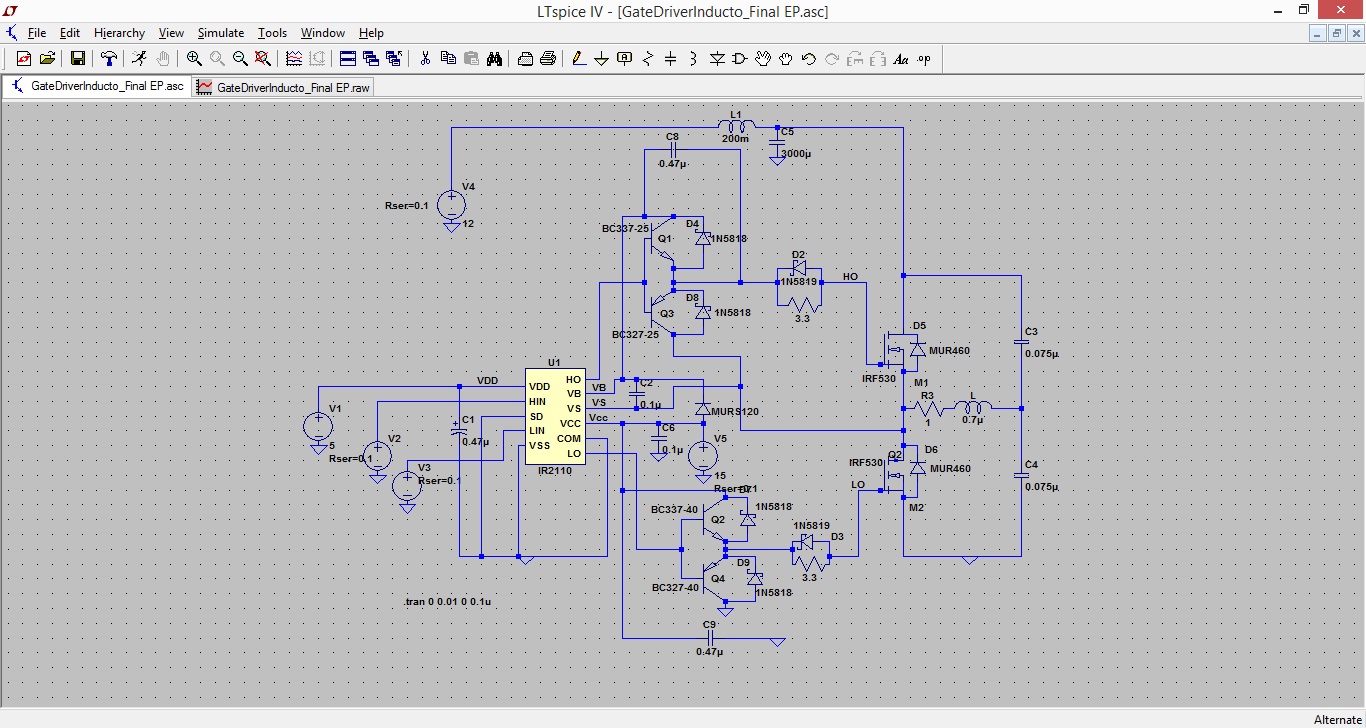
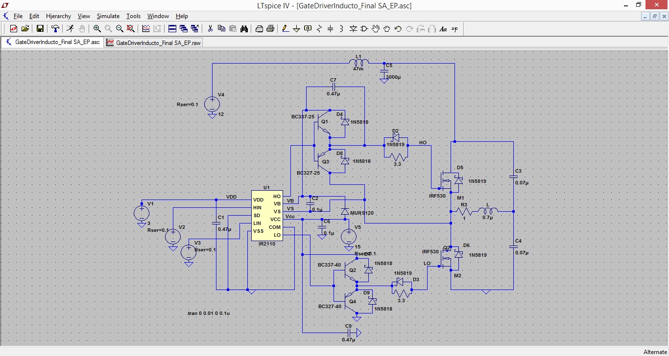
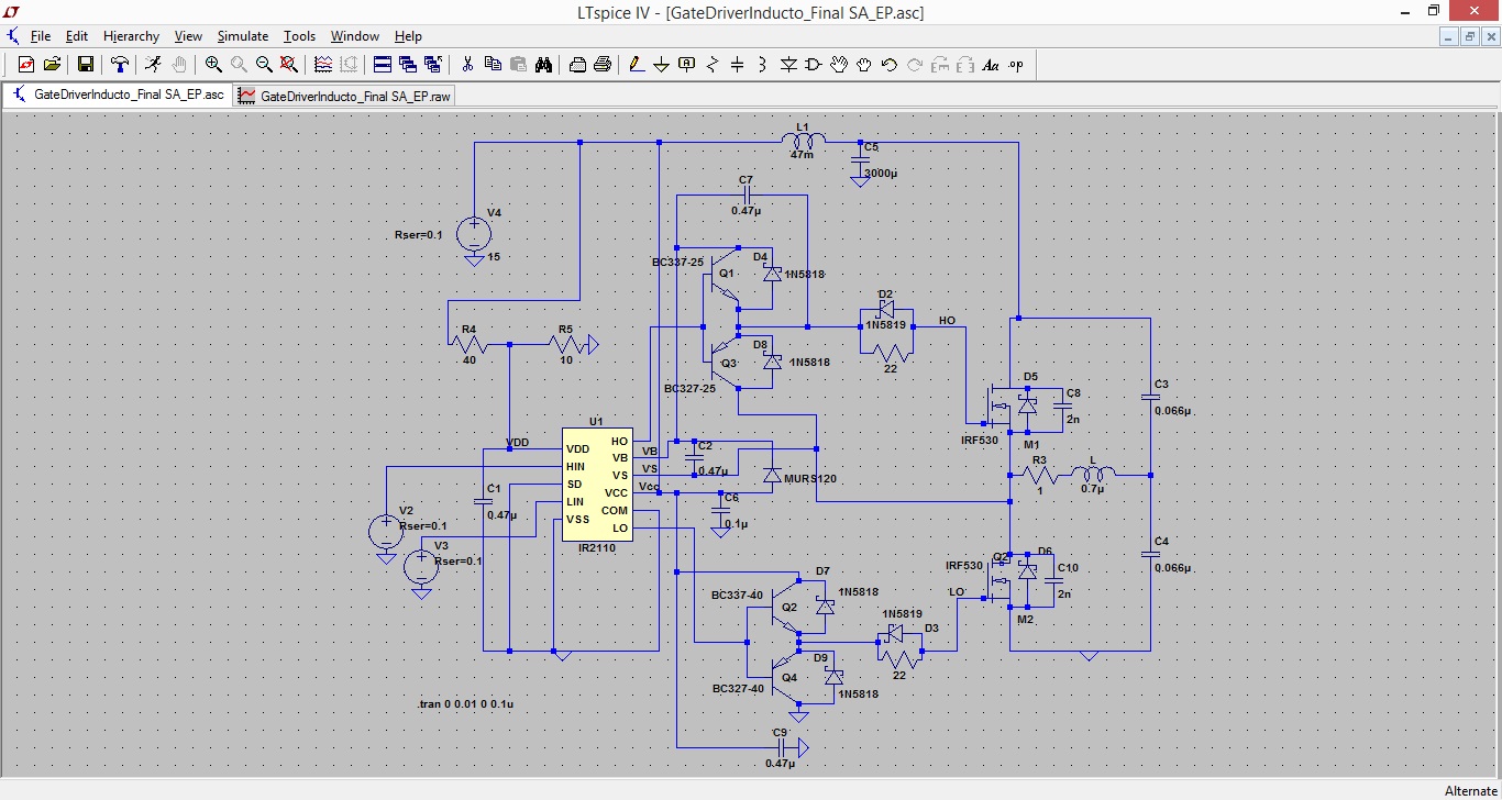
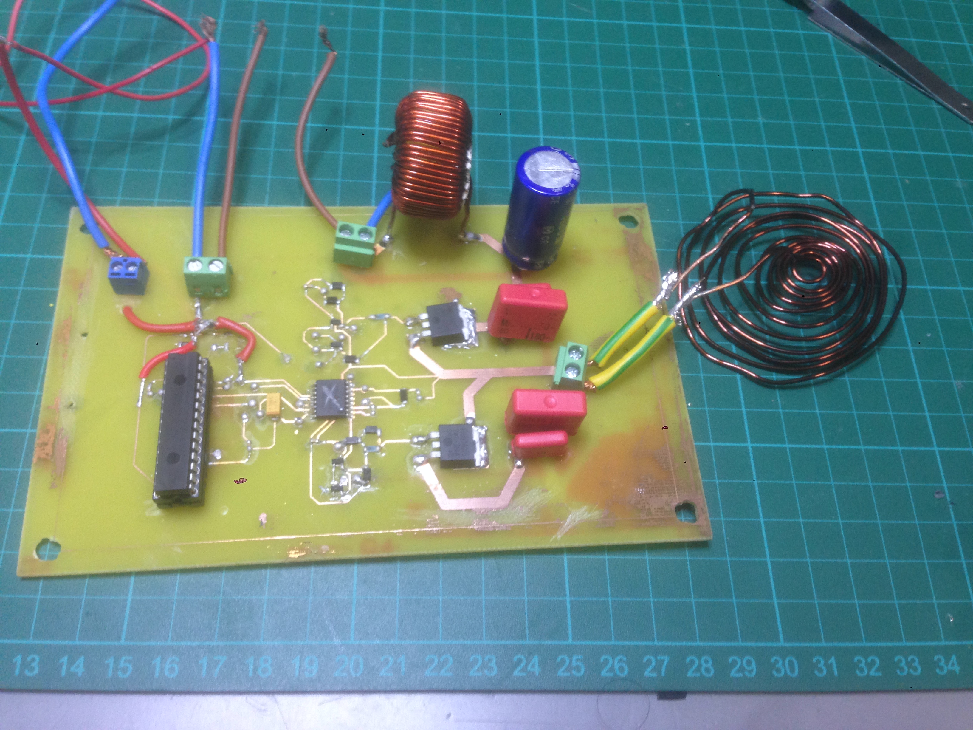
can you post your corrected schematic?

- - - Updated - - -

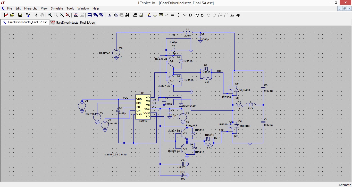
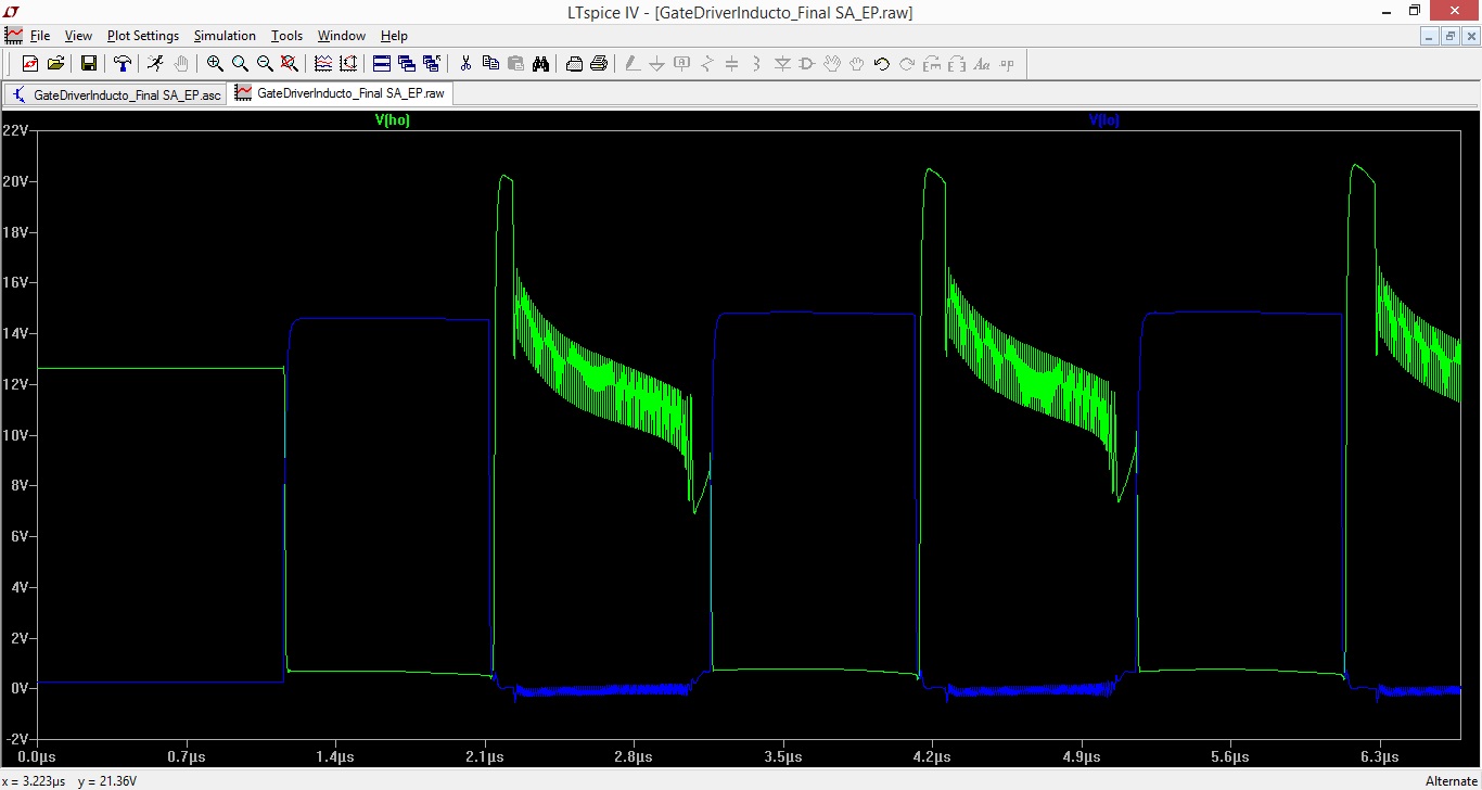
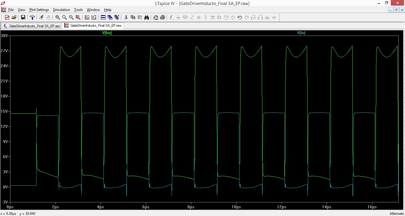
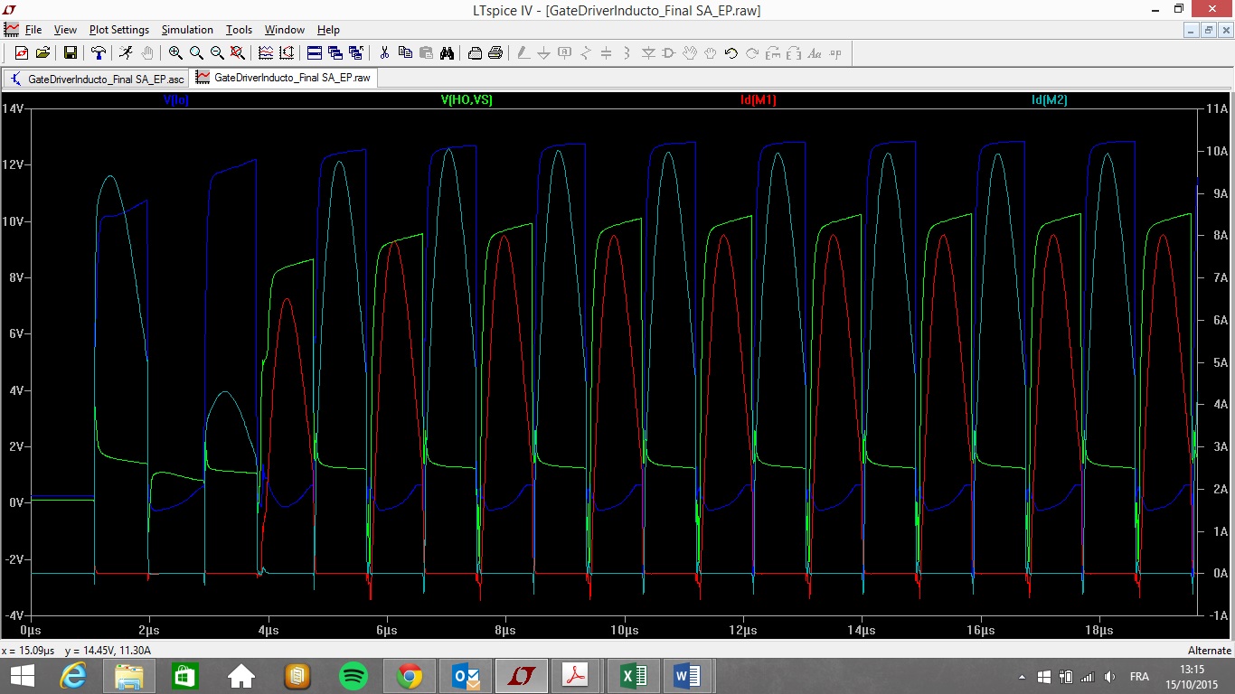
Delete C7, C10 in your sim...

- - - Updated - - -

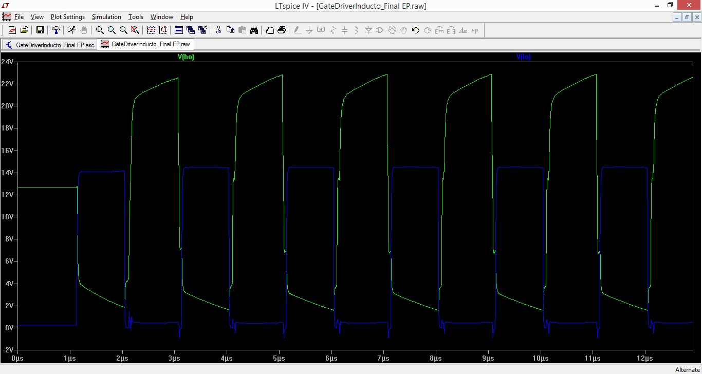
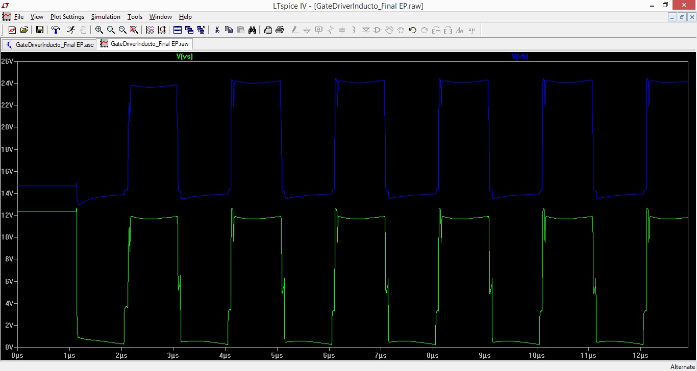
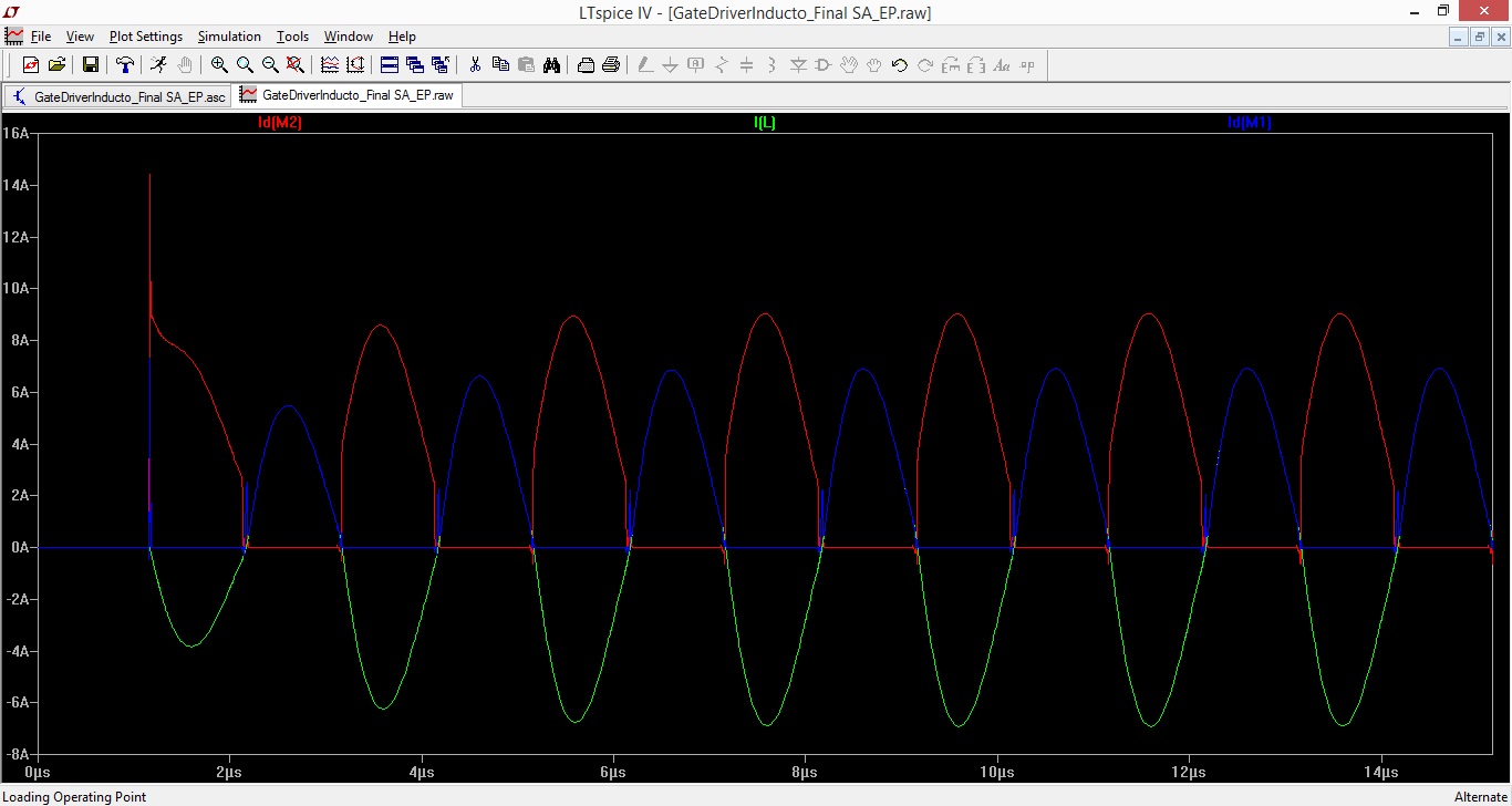
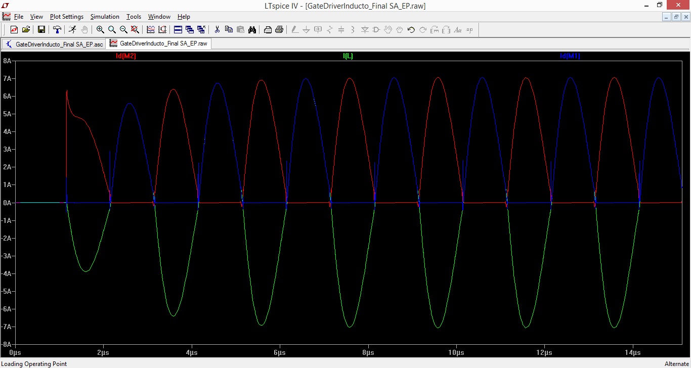
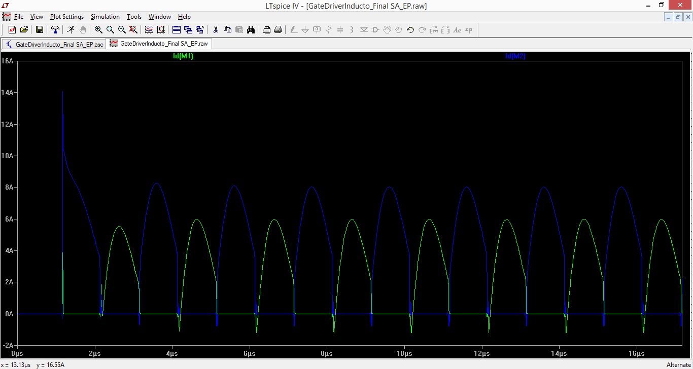
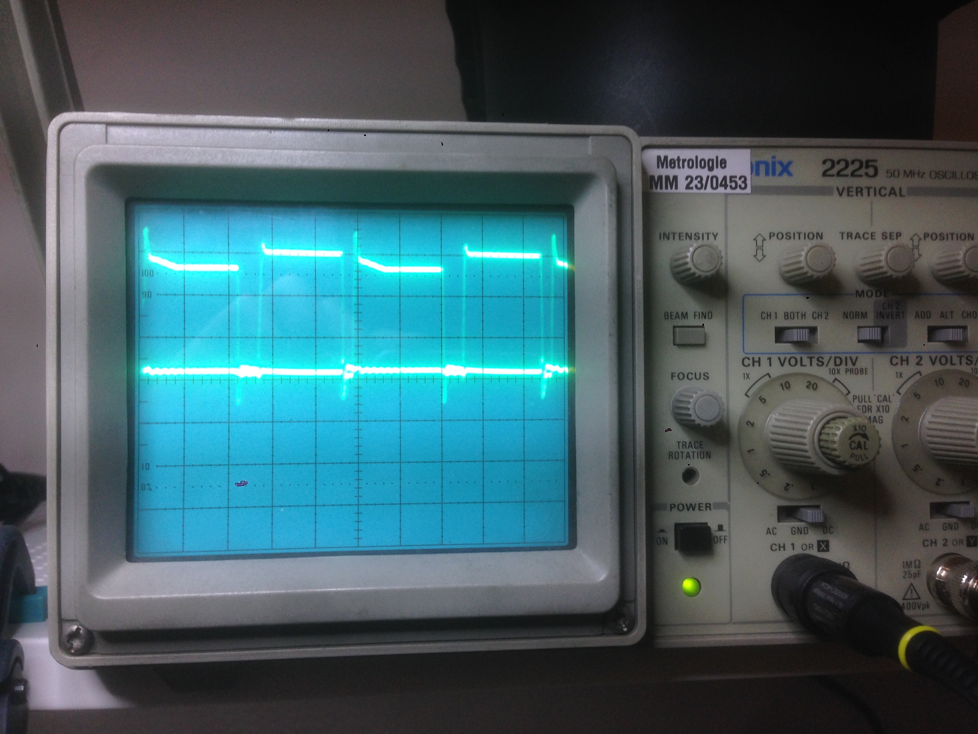
and vary the freq until things look right, there is only one freq where the circuit is single cycle resonant - you want to be just above that. 1.555MHz, or 1.04 MHz (1.5 rings of the power circuit) or, 778kHz, (2 rings of the power circuit)
 

I corrected the schematics according to your inputs.

Problem are that LO and HO are not equal anymore due to the fact that HO becomes influenced by the power rail. Which is not supposed to happen. If I increase V4, HO increase as well...
Modifying the frequency signals doesn't improve things.


- - - Updated - - -

Here's my schematics version

The only issue is that HO is quite disturbed and the simulation slow. But the rest seems fine.
What do you think of this schematics and simulation ?

- - - Updated - - -


Ho looks correct, the gate drive has to go higher than the power rail, to drive the fet when it is on, i.e. low volts across it.

there is some osc on the green signal that needs sorting
 

Things are starting to look fine !
The question is on C7 and its impact on the results depending on it is wired or even on the design.

If it is connected on HO, then the results are fine. Only the current in the fets have a kind of offset. This might create losses in the fets and heat that may lead to failure... I am trying a soft switching of the gates.


- - - Updated - - -

But If I remove C7... no more offset ! Results are very good.


- - - Updated - - -

If C7 is on GND... then HO tends to oscillate a lot !


Put C7 back where it was, you need to add more parasitic R to limit the oscillations, your circuit is too "perfect"
 

Put C7 back where it was, you need to add more parasitic R to limit the oscillations, your circuit is too "perfect"

Okay.

So I keep C7 on HO. And add parasitic R. Anywhere ? Or should it be specific ?
 

Which oscillation are you refering to ? HO oscillation (green) when it is high ?

The thing that I don't get is why the current in the high fet and the low fet are not equal.
Id (M2) starts higher which doesn't affect the current in the inductor (nice sinusoidal wave).


I did add resistance on all capacitors.
 

Geez, the osc is plain to see, the currents start differently due to your start conditions in the sim, if you let it run for much longer they will equalize, you can see this if you look more closely at what you have posted.... more parasitic R to reflect the real world would help too...
 
  • Like
Reactions: Sadek

    Sadek

    Points: 2
    Helpful Answer Positive Rating
If you look at Vgs (green signal) than no more osc !


- - - Updated - - -

Easy Peasy, I have a question concerning the power supply.

Is there any risk if i connect the main power source to the IR2110 and to the power rail ?
I am concerned that too much current may flow to the IR2110 and burn it. Should I add any current protection or limiter in between even if it is the same voltage level ?
 

Final ?

I need 3v for VDD and 15V for Vcc. Vmain will be 15.


It might work, depending on the current drawn by the chip at your operating freq...
 
  • Like
Reactions: Sadek

    Sadek

    Points: 2
    Helpful Answer Positive Rating
C7 is still wrong...

- - - Updated - - -

why not have -40 xtors for Q1, Q3?
 
  • Like
Reactions: Sadek

    Sadek

    Points: 2
    Helpful Answer Positive Rating
Ok for C7.

-40 xtor ? What It is ?
I was about to select it considering mainly current and frequency.

I worked on the PCB design. An Fairchil application note explains that Rg and the gate driver should be as close as possible to the gate drive pin. I imagined the opposite since the high power high frequence induction would create interference and potentiel noise.

Any additional recommendations ?
 

-40 same as Q2, Q4

Keep all gate drive loops small and track lengths short, de-coupling caps close to active circuits.
 
  • Like
Reactions: Sadek

    Sadek

    Points: 2
    Helpful Answer Positive Rating
Sorry but I don't know what you mean by "-40". What is it exactly ?
 

look at Q2, Q4 you've already used -40 xtors in your sim...
 
  • Like
Reactions: Sadek

    Sadek

    Points: 2
    Helpful Answer Positive Rating
Hello everyone !!

Designed the layout and produced the PCB... and the results are yet to be convincing...
I managed to solve all issues apart from one.

When I measure the signal on the fets gate without the power on, the signal is clean square wave.


When I turn the power on, then the signal gets all noisy. The only way to solve this issue is to use coax cable between the gate driver and the fets gate. I don't know where the problem comes from. I checked induction cooker and the driver is connected directly to the IGBT though the PCB.
 

Anyone has any idea how I could fix this issue ? or where it's from ? ground short loops ? Any leads ?
I reduced the frequency down to 100kHz.
 

Status
Not open for further replies.

Similar threads

Part and Inventory Search

Welcome to EDABoard.com

Sponsor

Back
Top