Continue to Site

Welcome to EDAboard.com

Welcome to our site! EDAboard.com is an international Electronics Discussion Forum focused on EDA software, circuits, schematics, books, theory, papers, asic, pld, 8051, DSP, Network, RF, Analog Design, PCB, Service Manuals... and a whole lot more! To participate you need to register. Registration is free. Click here to register now.

IR2110 C1 charging current problem

Status
Not open for further replies.

tyilgin

Junior Member level 2
Joined
Jul 9, 2010
Messages
23
Helped
0
Reputation
0
Reaction score
0
Trophy points
1,281
Activity points
1,504
Hi,

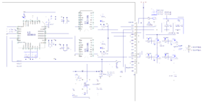
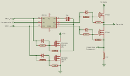
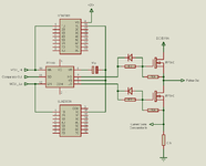
I am trying to apply the diagram in the picture, but due to the current drawn by C2 and C8 during charging, the voltage formed on the 0.1r value R24 that feeds the low mosfets, Although it is delayed with the 1000pf value C21, it is noticed with the LM393 and a overcurrent alarm is created.

I'm trying to separate this situation from the true short circuit and overcurrent situation.

For this purpose, I plan to manage the charging and discharging of the VS(Pin 6) pin and the C1 capacitor over these mosfets by placing a small mosfet on the LIN(Pin 12) and HIN(Pin 14) inputs of the Ir2110.

Do you think this schematic that I designed with mini mosfets in the Sot23 case makes sense ?
If it makes sense, should it be used with the IRF840 at the input or output of the IR2110 ?

If you have any other suggestions, I would be very grateful.
 

Attachments

  • 6-5 _.png
    6-5 _.png
    915.3 KB · Views: 106
  • Ornek.png
    Ornek.png
    41.6 KB · Views: 98

Your circuit ignores the necessity to connect Vs to high-side source as return for the gate driver voltage. It can't work.

I would try a series resistor to bootstrap diode to reduce charging peak current.
 

Hi,

I don't think this is a good approach....

But let's use it:
You built a power halfbridge (better say: two) by two N-Ch Mosfets... and need a driver IC with bootstrap circuit to drive the high side Mosfet gate with enough voltage...

Now you built a "low power" half bridge with two N-Ch Mosfets ... but without proper high side driver
Why? The same rules for voltages apply to the low power halfbridge.
--> You need a proper high side driver.

*******

But like already said, I don't see the benefit.
Do you have a scope to verify your current sense voltages?

In my eyes the low side gate drive current, as well as the bootstrap charging current are (known) errors to the ccurrent measurement.
Both currents are rather constant, thus they can be "calibrated out".
Both currents are short in time peaks and can be attenuated a lot.

Additionally both currents timing is known, thus you could "gate them out" with an analog switch at the sense line.

More advanced solutions are to design a "compensating RC network" that generates similar waveform pulses as the erroneous current and subtract them at the sensor line. But indeed I think this is overkill.

A clean approach for a solution is:
* clearly define in timing and magnitude, accuracy and tolerance how your current measurement should work. (Define where you want to go)
* clearly find out the errors in magnitude and timing (know your enemy)

Only when both values are known one can find a good solution.
Also it helps to find out that maybe the error you see is not caused by what you think the error source is.
Sometimes then the solution is rather simple, like:
* adding a second order filter ... adjusting cutoff frequency .... to the current measurement.

But in your case there may be other error sources:
* bad PCB layout --> improve the PCB layout
* shunt with too high series impedance (like wire wound resistors) --> use a more suitable shunt
* ground bouncing --> use kelvin wiring for current measurement
* ...

Klaus
 

Your circuit ignores the necessity to connect Vs to high-side source as return for the gate driver voltage. It can't work.

I would try a series resistor to bootstrap diode to reduce charging peak current.
I don't think it would be right to charge the C1 outside of the charge/discharge time in an external way. If you mean only feeding at charging time, the problem during discharge comes to light at this time, I also have protection in the Hi direction :(

Thank you very much for your reply.
 

Hi,

I don't think this is a good approach....

But let's use it:
You built a power halfbridge (better say: two) by two N-Ch Mosfets... and need a driver IC with bootstrap circuit to drive the high side Mosfet gate with enough voltage...

Now you built a "low power" half bridge with two N-Ch Mosfets ... but without proper high side driver
Why? The same rules for voltages apply to the low power halfbridge.
--> You need a proper high side driver.

*******

But like already said, I don't see the benefit.
Do you have a scope to verify your current sense voltages?

In my eyes the low side gate drive current, as well as the bootstrap charging current are (known) errors to the ccurrent measurement.
Both currents are rather constant, thus they can be "calibrated out".
Both currents are short in time peaks and can be attenuated a lot.

Additionally both currents timing is known, thus you could "gate them out" with an analog switch at the sense line.

More advanced solutions are to design a "compensating RC network" that generates similar waveform pulses as the erroneous current and subtract them at the sensor line. But indeed I think this is overkill.

A clean approach for a solution is:
* clearly define in timing and magnitude, accuracy and tolerance how your current measurement should work. (Define where you want to go)
* clearly find out the errors in magnitude and timing (know your enemy)

Only when both values are known one can find a good solution.
Also it helps to find out that maybe the error you see is not caused by what you think the error source is.
Sometimes then the solution is rather simple, like:
* adding a second order filter ... adjusting cutoff frequency .... to the current measurement.

But in your case there may be other error sources:
* bad PCB layout --> improve the PCB layout
* shunt with too high series impedance (like wire wound resistors) --> use a more suitable shunt
* ground bouncing --> use kelvin wiring for current measurement
* ...

Klaus
I think it may be to clip the first moments of charge and discharge times with a switch, but unfortunately it is not fast enough to do this since I am working with PIC18F452 (40Mhz). I can only create a 30-70hz ac sine with 0.1hz resolution.

My circuit paths are far and short distance from other factors. It is also grounded with a copper filler around it. So I don't think I have other sources of error. This issue, which I overlooked because I did not spend much time on the current protection part on the prototype board, is now looking at me like a giant iceberg.

I strengthen the voltage falling on 0.1r with an opamp and enter the 74HC4078 (8 Input or gate) with the ones coming from the hi side.
The output feeds the SD inputs of the IR2110.

Also, the voltages coming from the opamp at the input of the 74HC4078 are read with the pic18f452, trying to catch overcurrent or disconnection.

Since most of the work I have done so far is on digital electronics (a bit of my lack of knowledge, of course), I started looking for a logical solution and I have been waking up for a few days. But I guess there seems to be no choice but to find the appropriate combination of R7 and C21 in the diagram.

Thank you very much for taking the time to comment.
--- Updated ---

Hi,

I don't think this is a good approach....

But let's use it:
You built a power halfbridge (better say: two) by two N-Ch Mosfets... and need a driver IC with bootstrap circuit to drive the high side Mosfet gate with enough voltage...

Now you built a "low power" half bridge with two N-Ch Mosfets ... but without proper high side driver
Why? The same rules for voltages apply to the low power halfbridge.
--> You need a proper high side driver.

*******

But like already said, I don't see the benefit.
Do you have a scope to verify your current sense voltages?

In my eyes the low side gate drive current, as well as the bootstrap charging current are (known) errors to the ccurrent measurement.
Both currents are rather constant, thus they can be "calibrated out".
Both currents are short in time peaks and can be attenuated a lot.

Additionally both currents timing is known, thus you could "gate them out" with an analog switch at the sense line.

More advanced solutions are to design a "compensating RC network" that generates similar waveform pulses as the erroneous current and subtract them at the sensor line. But indeed I think this is overkill.

A clean approach for a solution is:
* clearly define in timing and magnitude, accuracy and tolerance how your current measurement should work. (Define where you want to go)
* clearly find out the errors in magnitude and timing (know your enemy)

Only when both values are known one can find a good solution.
Also it helps to find out that maybe the error you see is not caused by what you think the error source is.
Sometimes then the solution is rather simple, like:
* adding a second order filter ... adjusting cutoff frequency .... to the current measurement.

But in your case there may be other error sources:
* bad PCB layout --> improve the PCB layout
* shunt with too high series impedance (like wire wound resistors) --> use a more suitable shunt
* ground bouncing --> use kelvin wiring for current measurement
* ...

Klaus
Your comment on switching has sparked a new idea.

Can this technique be used, or should the VS pin of the IR2110 be connected to absolute 2 mosfets?
 

Attachments

  • 2.png
    2.png
    43.2 KB · Views: 96
Last edited:

Your comment on switching has sparked a new idea.

Can this technique be used, or should the VS pin of the IR2110 be connected to absolute 2 mosfets?
Sorry for bullshit as a result of my insomnia, This situation is no different than before...
 

Status
Not open for further replies.

Similar threads

Part and Inventory Search

Welcome to EDABoard.com

Sponsor

Back
Top