Continue to Site

Welcome to EDAboard.com

Welcome to our site! EDAboard.com is an international Electronics Discussion Forum focused on EDA software, circuits, schematics, books, theory, papers, asic, pld, 8051, DSP, Network, RF, Analog Design, PCB, Service Manuals... and a whole lot more! To participate you need to register. Registration is free. Click here to register now.

IR2109 Gate Drive Issue

Status
Not open for further replies.

adnan012

Advanced Member level 1
Joined
Oct 6, 2006
Messages
468
Helped
2
Reputation
4
Reaction score
2
Trophy points
1,298
Visit site
Activity points
4,923
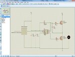
I am working on a half_Bridge as shown in the attached file.

20KHZ PWM is generated by PIC18F4550. PWM signal is fed to Opto coupler FOD3120.
Micro controller and FOD3120 input side have separate ground.

FOD3120 output side is connected to the IR2109 (gate driver). Opto coupler (output side) , Gate Driver and IGBT have same ground.

Micro-controller is programmed to generates PWM (20KHz) with a duty of 10%. After every second duty cycle is incremented with a 5% step and reaches to 90% duty. The motor works fine during this period. it draws 1 amp current under no load conditions.

On oscilloscope i can verify the gate signals on both igbt' gates. 14 -15 volt at the gate of the lower IGBT and (28+ 15- vf) = 42 volts with respect to system ground. These Gate voltage are valid for all Duty cycles.

But when the micro-controller starts decreasing duty cycle in the same manner (90% to 10% with 5% decrement after every second) the gate voltage at the high side igbt fluctuates. And the gate drive ic is damaged. However IGBTs, opto-coupler and controller are safe

So far i have burned 2 driver ic. I need help to sort out the issue.

IR2109 output current limit is 120 mA / 250 mA. What is the peak gate current required to drive IGBT ?
 

Attachments

  • HalfBridge_Motor_Driver.JPG
    HalfBridge_Motor_Driver.JPG
    70.2 KB · Views: 309
  • FOD3120.pdf
    407.5 KB · Views: 151
  • ir2109.pdf
    350.3 KB · Views: 123
  • irg4pc50w.pdf
    159.7 KB · Views: 159
  • mbrd320.pdf
    182.9 KB · Views: 136

Does it immediately die after the first 5% reudction (i.e. 90% -> 85%) ? or it takes longer? If so, what duty-cycle?

Since the IGBTs aren't dying, I assume the gate-driver cannot for some reason cope with the negative voltage generated by reaction of your inductive load (motor) when the voltage across the motor is being reduced due to reduction in Duty-Cycle (V(S) falling below -25V relative to V(B)).

I would also be interested to see a o'scope shot across C2. Also, what is the C2 Voltage Rating? I hope it's more than 50V?
 
Thanks for reply.

Driver was damaged after 5 to 10 second. At this point the duty cycle was below 50%.

I need to buy chips for further experiments.

I am not sure about the voltage rating of C2. I need to verify it . i by mistake mixed 50 and 100 volts capacitors.
 
Last edited:

Whether C2 is rated at 50V or 100V should be irrelevant to the problem you are having. The maximum voltage across C2 at any given time should only be VCC minus Vf of D1, so using the values in your schematic, 15v(VCC) - 0.49v(Vf of D1) = 14.51v

When the high-side IGBT is switched on, this will raise the Vs side of C2 to ~+28VDC in reference to GND, that in turn will push the Vb side of C2 up to ~+43VDC, again, in reference to GND, but it's the voltage across the cap that matters, which with a properly functioning bootstrap setup should never be able to exceed the VCC rail.

-Brad
 
I think the circuit what you are using is a very basic one with no protection at the IGBT driver IC output driver pins. The transients coming from the load - the motor have to be suppressed before they reach the IGBT driver pins. You may want to try some protection circuit for the IGBT driver pins similar to the circuit in this application note - AN889, VF Control of 3-Phase Induction Motors Using PIC16F7X7 Microcontrollers from Microchip. Refer page # 18.
 
I think the circuit what you are using is a very basic one with no protection at the IGBT driver IC output driver pins. The transients coming from the load - the motor have to be suppressed before they reach the IGBT driver pins. You may want to try some protection circuit for the IGBT driver pins similar to the circuit in this application note - AN889, VF Control of 3-Phase Induction Motors Using PIC16F7X7 Microcontrollers from Microchip. Refer page # 18.

I would have to agree with this. At the very least, you should have free-wheeling diodes across the IGBTs.
 
Thanks for reply.

I am using DSEI120-12A as freewheeling diode across each IGBT (IRG4PC50W).
What is the proper technique to protect Gate Driver IC?
How motor transients can be suppressed before reaching to the gate driver IC?
 

In my opinion addition of TVS diode and a capacitor between G and E would be good. This TVS diode will suppress and voltage as well as the current transients. The cap can handle smaller transients and also act as a smoothing capacitor with the TVS. Again, I am referring some links here for you so that you can take an informed call on how to implement the protection circuit.

**broken link removed**
 
I have arranged p6ka18 TVS diode for the protection of the IGBT gate.
Which capacitor value should i use between gata and source?
 

In my opinion addition of TVS diode and a capacitor between G and E would be good. This TVS diode will suppress and voltage as well as the current transients. The cap can handle smaller transients and also act as a smoothing capacitor with the TVS. Again, I am referring some links here for you so that you can take an informed call on how to implement the protection circuit.

Maybe gate to source capacitance act as smoothing but however the bootstrap capacitor do the same task actually it connects between your bridge's emmitter(or source when using nmos) and gate.

I've just finished my 3 phase motor driver circuit. I want to help you when seeing your topic cause i was struggle with the bootstrap capacitor.

Firstly, when you decide to drive your fets or igbts with using bootstrap method, you actually can not reach at %100 duty theoratically because, when %100 duty signal act as dc so it can not charge your bootstrap capacitor properly. I writed a matlab code for calculating bootstrap capacitor minimum value in related to almost every parameter even bootstrap capacitor leakeage current. I changed its parameters suited with your igbt's total gate charge and frequency etc. Eventually, your required value for bootstrap capacitor is approximately minimum 0.7uF. However, in my opinion you should use 2.2uF to 4.7uF electrolytic capacitor which voltage rating is above your supply voltage of gate driver which is 15V. Also, you should use 0.1nF ceramic capacitor parallel to bootstrap for filtering high frequency components.

Also, you should measure the capacitor charging current which should be desirable level in related to your frequency. Maybe, you have to use bootstrap resistor to limit your charging current whose value is a few ohms.

The other thing you should consider is that you should put a resistor whose value is 1k or maybe higher between gate to emmitter for high switch igbt and gate to ground for lower one. It is used for decharging the gate current in the case of unwanted gate charge while starting-up.

If your gate drivers output current is not enough to drive igbt' gate. You should use totem-pole structure in front of the output to feed the current.

I am sending to you my matlab code maybe you want to change any variables to see the variation of bootstrap capacitor value.

Hope it helps.
 

Attachments

  • adnan012_bootstrap_capacitor_calculation.rar
    893 bytes · Views: 116
Gate-source capacitors are not commonly used for low-voltage IGBT (< 3kV). They are suggested in some application notes for switching optimization but would never be required. Quite surely they are not the solution for your problem. TVS diodes aren't bad, although I don't believe that they are required here. Would be different in case of IGBT damage.

All-in-all it's still mysterious how you manage to burn the drivers. A possible problem could be severe undershoot of the bridge output node, which might happen with bad circuit layout. There are suggestions of series resistors to handle undershoot problems in IRF application notes.
 
hi,

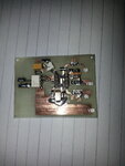
i have designed the gate driver daughter card PCB. Now the driver ic IR2109 is safe during testing.
 

Attachments

  • Gate_Driver_Daughtert Card.jpg
    Gate_Driver_Daughtert Card.jpg
    2.1 MB · Views: 162

Status
Not open for further replies.

Similar threads

Part and Inventory Search

Welcome to EDABoard.com

Sponsor

Back
Top