Welcome to our site! EDAboard.com is an international Electronics Discussion Forum focused on EDA software, circuits, schematics, books, theory, papers, asic, pld, 8051, DSP, Network, RF, Analog Design, PCB, Service Manuals... and a whole lot more! To participate you need to register. Registration is free. Click here to register now.
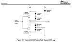
The parasitic diodes are inherent to the FET's structure. The point where the diodes meet is the body of the FET, and this node must be biased somewhere for proper operation. Normally the body node is connected directly to the source of the FET, which in a CMOS circuit will be either GND or Vcc. This is the case for the N channel FET in your schematic. One of its parasitic diodes is effectively short circuited, and does nothing. But for the P channel FET here they put an extra diode in series to Vcc in order to prevent excessive current flow from the output to Vcc.
Parasitic diodes should not be counted on for any current
circulating / shunting. They may (depending on construction)
inject substrate current causing latchup above some weakly
specified threshold, or may just corrupt analog circuitry.
This site uses cookies to help personalise content, tailor your experience and to keep you logged in if you register.
By continuing to use this site, you are consenting to our use of cookies.