Continue to Site

Welcome to EDAboard.com

Welcome to our site! EDAboard.com is an international Electronics Discussion Forum focused on EDA software, circuits, schematics, books, theory, papers, asic, pld, 8051, DSP, Network, RF, Analog Design, PCB, Service Manuals... and a whole lot more! To participate you need to register. Registration is free. Click here to register now.

input common mode and differential capacitance extraction for an op-amp

Status
Not open for further replies.

Junus2012

Advanced Member level 5
Joined
Jan 9, 2012
Messages
1,552
Helped
47
Reputation
98
Reaction score
53
Trophy points
1,328
Location
Italy
Activity points
15,235
Hello all

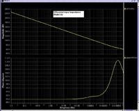
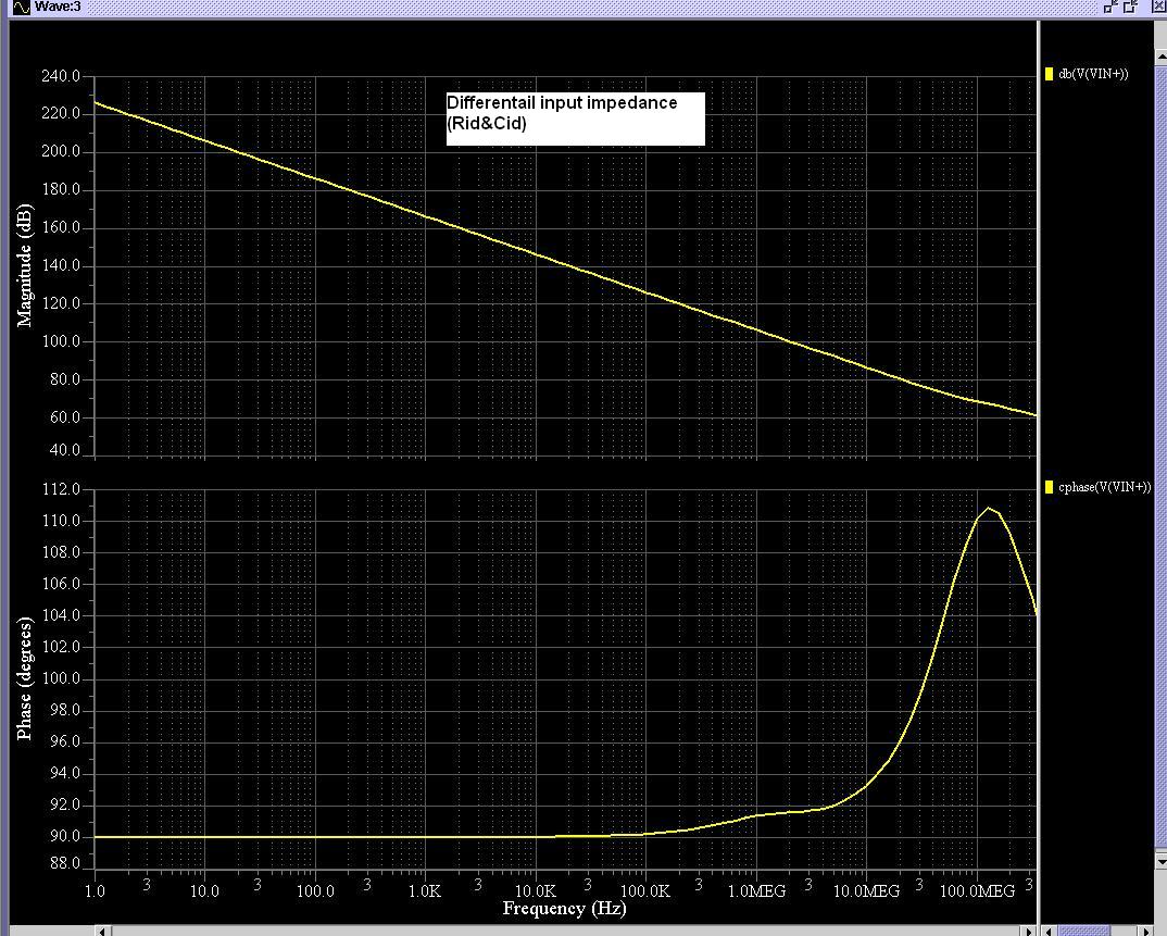
I am trying to simulate the input differential resistance and capacitance for my operational amplifier.
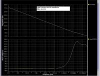
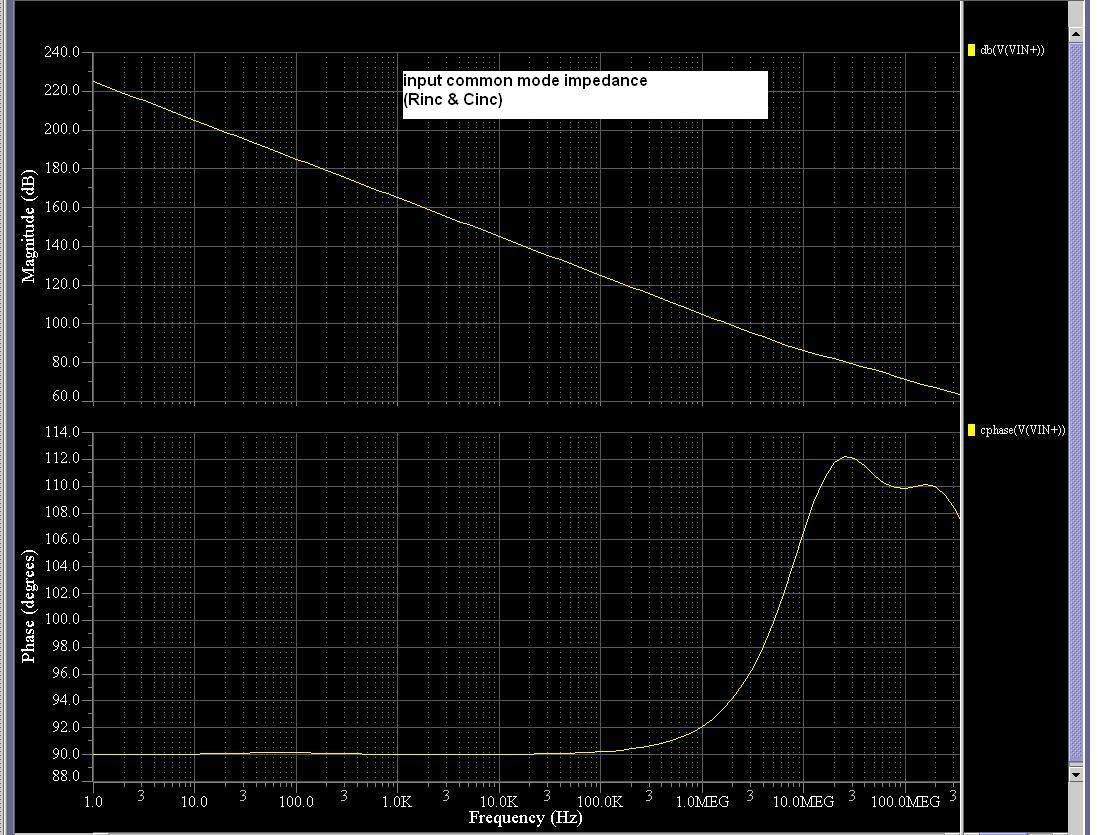
I am also trying to simulate the common mode input resistance and capacitance.

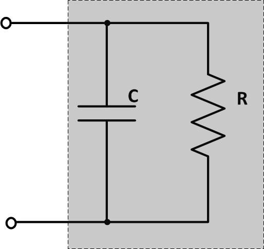
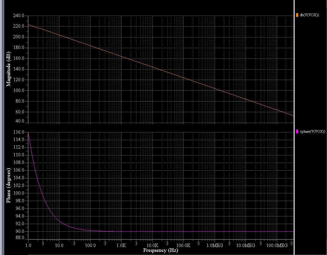
I assumed that both of the resistance and the capacitance are in parallel, so I connected a current source and I run the AC simulation. I got theses two result but it seems al little strange for me


I am looking for your help

Regards
 

1. Seeing a phase of +90° for a capacitiv impedance seems to indicate wrong measurement polarity.

2. The impedance plot suggests, that the equivalent circuit is not a RC parallel circuit. There's apparently a series R to the cpacitor that get's effective at higher frequency. Technically, this would be at least expectable.

3. You are talking about simulation. Seeing the simulation circuit will most likely help to understand what's going on.
 

Dear FvM

I have assumed the parallel connection after I read about the input resistance and capacitance from texas Instruments, I attached you the document, please refer to page 31
 

Attachments

  • sseZo.pdf
    367.8 KB · Views: 97

Still open simple question, which circuit are you simulating?

The TI paper doesn't specifically address input impedance at > 10 MHz. It will be obviously affected by input stage common and differential mode bandwidth and gate/base bulk resistances.
 

I am simulating both the differential and common mode input resistance and capacitance exactly as the documents talked about it. if you it again, you will find that always talking about total resistances and capacitances are in parallel. I will tell you according to that how I did the simulation:

1. in finding the input common mode resistance and capacitance, I shorted the both terminal of the op-amp after I applied the necessary offset voltage. I connected an AC current source at the input then I run the AC analyses for wide range frequency, the voltage that I probed is from the input itself.

2. in finding the input differential capacitance and resistance, I grounded the inverting terminal and I repeated the same previous simulation as you in the second graph

here, is the equivalent impedance circuit fgor both cases


Still open simple question, which circuit are you simulating?

The TI paper doesn't specifically address input impedance at > 10 MHz. It will be obviously affected by input stage common and differential mode bandwidth and gate/base bulk resistances.
 

1. Seeing a phase of +90° for a capacitiv impedance seems to indicate wrong measurement polarity.

As the stimulus is a current, I think this is ok for a purely capacitive impedance. The (parallel) resistive input impedance could only be seen at much lower frequencies, I'd think.
 

Mr. erikl

I think you want to say at higher frequency, because at low frequency the resistance is very high and it is approxiametly open circuit.

As the stimulus is a current, I think this is ok for a purely capacitive impedance. The (parallel) resistive input impedance could only be seen at much lower frequencies, I'd think.
 

As said in post #2, it's obvious that the simulated OP shown th eimpedance plot in post #1 can't be represented by a parallel RC circuit in post #5.

You still didn't tell what's the actually simulated circuit. (e.g. a transistor level OP model with MOS or BJTinput stage, an OP macro model,....).

As the stimulus is a current, I think this is ok for a purely capacitive impedance.
The voltage across the capacitor will lag the current, in other words should show a phase of -90 degree.
The (parallel) resistive input impedance could only be seen at much lower frequencies, I'd think.
Yes.
 

Dear FvM

I am simulating a CMOS current mirror OTA with all MOS transistors. I am simulating with the transistor level.

I have tried a lot to find another method for simulating these parameters, but since it is not that important for many of the designers therefore I didnt find a specific other method to simulate it

thank you

As said in post #2, it's obvious that the simulated OP shown th eimpedance plot in post #1 can't be represented by a parallel RC circuit in post #5.

You still didn't tell what's the actually simulated circuit. (e.g. a transistor level OP model with MOS or BJTinput stage, an OP macro model,....).


The voltage across the capacitor will lag the current, in other words should show a phase of -90 degree.

Yes.
 

I am simulating a CMOS current mirror OTA with all MOS transistors. I am simulating with the transistor level.
In this case, input impedances as shown in post #1 are expectable. You see purely capacitive behaviour up to 100 kHz and almost up to 1 MHz. Above this frequency, various transistor impedances become effective.

You get out what you put in - for a detailed analysis all circuit elements directly and indirectly connected to the input nodes must be considered. A real IC will expose additional parasitic iimpedances, by the way.
 
Thank you,
do you know a more precise method for simulating these parameters or you think my method is ok ???
 

Mr. erikl
I think you want to say at higher frequency, because at low frequency the resistance is very high and it is approxiametly open circuit.

No, at lower frequencies. Think twice: probably there will be a rather high parallel resistive part of the input impedance. At your test frequencies (> 1Hz), the capacitive share is already much less than the resistive part, so you can't see the latter one. Also, see FvM's confirmation.

- - - Updated - - -

The voltage across the capacitor will lag the current, in other words should show a phase of -90 degree.
Yes, you are right. So the polarity must be exchanged, as you told in post #2.
 
Dear FvM and erikl

I have simulated an ideal parallel capacitor and resistor. I have chosen the value of the resistor is very large to get the same response I got from the op-amp. I attached the simulation result here


As you see, the response is different from my first assumption (the input resistance and capacitance of the op-amp are in parallel as given in Texaxs Instruments document). it mean that the resistance and capacitance are not actually in parallel.
 

Here, again, you just see the capacitive share (1pF).
In order to see the resistive part of the input impedance, you have to start from much lower frequencies, where the phase still is 0°.
Instead of the magnitude, at the ordinate better plot the voltage (≘ resistance) directly - logarithmic scale is ok.
 

As you see, the response is different from my first assumption (the input resistance and capacitance of the op-amp are in parallel as given in Texaxs Instruments document). it mean that the resistance and capacitance are not actually in parallel.
Yes, I know. The parallel RC circuit is an appropriate equivalent circuit for a real OP, but not in the MHz frequency range. To model an impedance changing from pure capacitive to towards resistive with increasing frequency, you'll need a series RC circuit. But that's only the first order approximation. More circuit elements are required to represent the impedance characteristics shown in post #1.
 
Yes FvM, you were sure about that from your first reply.

And now, I am looking for a method for getting the values of these parameters by simulation, do you have an idea about that ??, I think you have, for sure :) :)

Yes, I know. The parallel RC circuit is an appropriate equivalent circuit for a real OP, but not in the MHz frequency range. To model an impedance changing from pure capacitive to towards resistive with increasing frequency, you'll need a series RC circuit. But that's only the first order approximation. More circuit elements are required to represent the impedance characteristics shown in post #1.
 

I'm not sure what you want to achieve. Your simulation "measurements" are showing diffential and single ende input capacitances of 0.8 respectively 8 pF (wrongly calculated, both are 0.8 pF). There will be in principle a parallel resistance, but it's not visible in the shown frequency range because Rp is apparently > 1e12 ohm. So the parallel RC circuit simplifies to C only for the 1 Hz to 100 kHz range.

You can try to find empirical equivalent circuits for the > 100 kHz frequency range, but I don't believe that it would be of much practical interest. If you want it though, a RC ladder network can be tuned to match an empirical impedance characteristic in the 0 to -90 degree range.

P.S.: See correction above.
 
Last edited:
Thank you FvM, no please I dont want it though :):)

I will follow your advice , but just tell me from the practical point of view, I see that this input capacitance is really large, do you think so or it is common in CMOS op-amp

Thanks alot

I'm not sure what you want to achieve. Your simulation "measurements" are showing diffential and single ende input capacitances of 0.8 respectively 8 pF. There will be in principle a parallel resistance, but it's not visible in the shown frequency range because Rp is apparently > 1e12 ohm. So the parallel RC circuit simplifies to C only for the 1 Hz to 100 kHz range.

You can try to find empirical equivalent circuits for the > 100 kHz frequency range, but I don't believe that it would be of much practical interest. If you want it though, a RC ladder network can be tuned to match an empirical impedance characteristic in the 0 to -90 degree range.
 

I see that this input capacitance is really large, do you think so or it is common in CMOS op-amp

With correction above and differential and common mode capacitance of 0.8 pF you're in a reasonable range. A real OP has most likely higher input capacitances because ESD protection and pad capacitances adds up.
 
Status
Not open for further replies.

Part and Inventory Search

Welcome to EDABoard.com

Sponsor

Back
Top