Continue to Site

Welcome to EDAboard.com

Welcome to our site! EDAboard.com is an international Electronics Discussion Forum focused on EDA software, circuits, schematics, books, theory, papers, asic, pld, 8051, DSP, Network, RF, Analog Design, PCB, Service Manuals... and a whole lot more! To participate you need to register. Registration is free. Click here to register now.

Inductive Current , High Current Track

Status
Not open for further replies.

azadfalah

Full Member level 2
Joined
Aug 13, 2016
Messages
145
Helped
1
Reputation
2
Reaction score
2
Trophy points
1,298
Activity points
2,423
Hi Friends,

The image below shows a power track ,12V - 24V , 50 amps and frequency 50 kHz
The track width is 10 mm
The chip shown in the image is SG3525

How do I calculate the proper distance from this track to place the SG3525? (To prevent destructive effects)
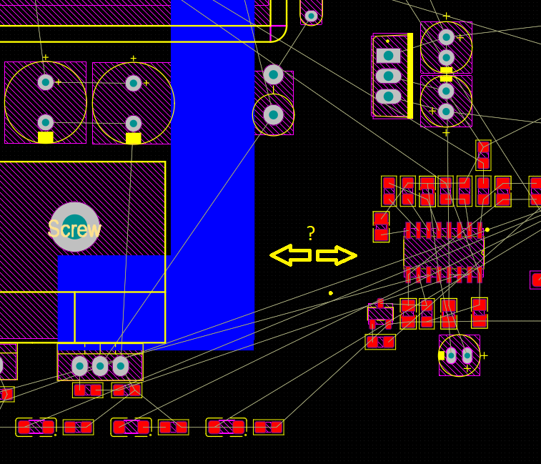
Power Track.png


Thanks a lot
 

Your trace is too narrow. How did you arrive at that 10mm value? Look at this :https://www.4pcb.com/trace-width-calculator.html . For 2 oz copper you should have 33mm.

you need to be concerned about distance between traces, not between traces and components.there are tables on the internet to select distance; it depends not only on voltage, but also environment.
 
i presume you are doing a switching converter. Its the "switching node" that you should keep away from ICs...or rather, keep away from sensitive traces......eg traces going into a comparator input, or an amplifier input, etc. It is the high dv/dt of switching nodes that is the killer in PCB layouts
--- Updated ---

dont for example, route a sensitive trace right over the top of switching node copper........sometiems you can interpose a "quiet node copper plane" in between the switching node and the sensitive trace, in order to shield the sensitive trace from the switching node.
--- Updated ---

..by "quiet node", i mean eg GND or Power plane copper...ie, something that is not being switched and bouncing up and down with high dv/dt
--- Updated ---

However, there are always exceptions, and as you see on page 16 of the following, the innoswitch control IC is situated right beneath the transformer, which obviously has a switching node going to it........and for some reason its ok in this case (its an offline flyback BTW)

**broken link removed**
 
Last edited by a moderator:
i presume you are doing a switching converter. Its the "switching node" that you should keep away from ICs...or rather, keep away from sensitive traces......eg traces going into a comparator input, or an amplifier input, etc. It is the high dv/dt of switching nodes that is the killer in PCB layouts
--- Updated ---

dont for example, route a sensitive trace right over the top of switching node copper........sometiems you can interpose a "quiet node copper plane" in between the switching node and the sensitive trace, in order to shield the sensitive trace from the switching node.
--- Updated ---

..by "quiet node", i mean eg GND or Power plane copper...ie, something that is not being switched and bouncing up and down with high dv/dt
--- Updated ---

However, there are always exceptions, and as you see on page 16 of the following, the innoswitch control IC is situated right beneath the transformer, which obviously has a switching node going to it........and for some reason its ok in this case (its an offline flyback BTW)

**broken link removed**
The OP was asking about “destructive effects“, not crosstalk.
 
The OP was asking about “destructive effects“, not crosstalk.
Yes, the original is rather vague.

Let's assume for a moment, he's actually talking about crosstalk, destructive may be read as a degree of severity, e.g. preventing correct operation of the circuit.
The OP is asking for a safe distance, the answer is: we don't know without considering the complete layout and the PCB stackup. If there's a continuous ground plane below the control circuit, you can place it quite near to the power trace. Also regarding inductive crosstalk, you don't look for individual high current traces, you look for commutation loops.
And I assumed he was talking about creepage distance. Regardless: creepage, crosstalk, the trace is too thin.
 

Dear Azadfalah, there is no easy / simple way to calc the distance to the IC to prevent interference - at least you have chosen one of the more robust ones, the 3525. To RFI proof your design I suggest you place 6 gnd pads around your IC to which you can solder small pcb pins such that you can then solder a small copper box around the IC ( top and bottom ) to reduce effects of generated RF noise getting onto the bond wires of the IC.

Further you can make sure the return path for your track is directly underneath ( or overtop ) the track - this will limit radiation

or - re-route it completely
 
Status
Not open for further replies.

Similar threads

Part and Inventory Search

Welcome to EDABoard.com

Sponsor

Back
Top