Continue to Site

Welcome to EDAboard.com

Welcome to our site! EDAboard.com is an international Electronics Discussion Forum focused on EDA software, circuits, schematics, books, theory, papers, asic, pld, 8051, DSP, Network, RF, Analog Design, PCB, Service Manuals... and a whole lot more! To participate you need to register. Registration is free. Click here to register now.

Induction heating problem

Status
Not open for further replies.

Mohamed.saleh

Newbie level 5
Newbie level 5
Joined
Apr 22, 2013
Messages
8
Helped
1
Reputation
2
Reaction score
1
Trophy points
1,283
Location
Egypt
Activity points
1,340
Recently I'm working on project of induction heating,,, I have H-bridge inverter, the mosfets which i am using is 20n60c3, my switching frequency is 1.5khz, i need to increase voltage level to as maximum as i could ,,, but i started experimenting with 30 Vdc over resistive load of 40 ohm, I was planning to reach 514V dc gradually but when i reach 30Vdc i am experimenting large current spikes over the resistive load, not to mention higher current and voltage spikes over inductive load of 11.3mH , the spikes appears at the transient of every half cycle. Current spikes are really so severe,, Dead band is 14 us, Any help please?
 
Last edited:

Recently I'm working on project of induction heating,,, I have H-bridge inverter, the mosfets which i am using is 20n60c3, my switching frequency is 1.5khz, i need to increase voltage level to as maximum as i could ,,, but i started experimenting with 30 Vdc over resistive load of 40 ohm, I was planning to reach 514V dc gradually but when i reach 30Vdc i am experimenting large current spikes over the resistive load, not to mention higher current and voltage spikes over inductive load of 11.3mH which is the coupling toroid, the spikes appears at the transient of every half cycle. Current spikes are really so severe,, Dead band is 14 us, Any help please?
Hi Mohamed
can you please show me your schematic ? with the exact value of each element ? thus i can find the problem however i can anticipate it but for a clear reply your schematic is required .
Best Wishes
Goldsmith
 

design.png
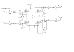
Here's schematic

optocoupler isolation signals 6n135 ,,
 

Try with high frequency isolated gate driver. did u consider dead time?
in ur ckt more possibilities are tre for shoot through. especially for high freq.

did u give enough space (gap b/w gate track and HV lines nearby) for gate line physically in H/W or nearby any HV line coming?

put the proper value of snubber ckt.
 

Hi Mohamed
Did you really used 670 ohms in series with gate of each mosfet ?? that is too large . reduce it as low as 10 ohms . and remove the diode and bjt transistor and then use a ferrite bead instead of them in series with the resistor in series with gate .
By the way use a diode in parallel with this composite system ! consider you have a ferrite bead in series with a resistor and in series with the gate . use a diode in parallel with that resistor and ferrite bead but of course cathode of the diode should be nearby side of your signal and it's anode should be tied into gate .
Do what i've told and then let me know the result . if the problem didn't removed then try to show me signals through your circuit . for example take signals of gates and GS of h sides . and signals across the each DS and signals across the load . and show me the picture of those signals . then i'll help you more .
Best Wishes
Goldsmith
 

Try with high frequency isolated gate driver. did u consider dead time?
in ur ckt more possibilities are tre for shoot through. especially for high freq.

did u give enough space (gap b/w gate track and HV lines nearby) for gate line physically in H/W or nearby any HV line coming?

put the proper value of snubber ckt.


I'm using already high freqency optocoupler,, 6n135 ,, and yes I have dead band 14us which is pretty much long time in my case. plus I only used 30Vdc till now with maximum output current on resistive load 3 ampere

- - - Updated - - -

Hi Mohamed
Did you really used 670 ohms in series with gate of each mosfet ?? that is too large . reduce it as low as 10 ohms . and remove the diode and bjt transistor and then use a ferrite bead instead of them in series with the resistor in series with gate .
By the way use a diode in parallel with this composite system ! consider you have a ferrite bead in series with a resistor and in series with the gate . use a diode in parallel with that resistor and ferrite bead but of course cathode of the diode should be nearby side of your signal and it's anode should be tied into gate .
Do what i've told and then let me know the result . if the problem didn't removed then try to show me signals through your circuit . for example take signals of gates and GS of h sides . and signals across the each DS and signals across the load . and show me the picture of those signals . then i'll help you more .
Best Wishes
Goldsmith

when i tried smaller resistance in range 100 ohm ,, the pluses distort and never gets to the Gate in square form,, my configuration assures that the pulses reach the gates in square for in perfect waveform,, but anyway I'll try your suggestions and I'll get you tomorrow when i go to the lab the pictures you requested,,
 
Last edited:

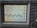
20130423_131508.png

upper waveform is the output voltage, and lower is the output current. as u can see ,, there's large spikes over the current,, it's measured over 0.1 ohm in series with 40 ohm load.

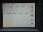
20130423_192944.png

that's the gate pulse for mosfet number 1 ,, and all pulses are well shape like that one.

20130423_192656.png

everytime I try to use smaller gate resistance as u recommended ,, voltage spikes appears.

N.B.: I don't have ferrite beads here in market.
 

it's measured over 0.1 ohm in series with 40 ohm load.
Hi again
Well , your voltages seems well , when the current is going like that we can be suspected that the sensing current resistor is the problem . what kind of resistor you've used to measure the current ? is that inductive ? i mean can you measure it's inductance by an LCR meter ? i think your resistor is very inductive . try to replace your sensing current resistor with a better one or use some resistors in parallel together and let me know the result . ok ?
Best Wishes
Goldsmith
 
Last edited:

I once tried to make an inverter from a transformer. I applied 12V AC square waves. I saw spikes at the transitions. I burned a few mosfets.

When you switch off heavy current through a coil, it creates high-V spikes.

When you break the circuit, the high-V can cause arcing. It may be a visible spark, or it may be between windings, or within components.

Solutions are not easy. It could be remedied by slowing the turn-off of the mosfet, but then you lose the advantage of operating it as a switch. It can overheat.

Snubber networks (diodes, capacitors, resistors, etc.) can help to a certain extent.
 

but for resistive load voltage and current waveform should be the same. only the amplitude of the waveform may get differ based on the resistor which we used to measure the current.

use current shunts to measure current. this will give very good and accurate result.

but still u can do some more modification in ur ckt to get good result.

use external highspeed diodes as like attached ckts

H-Bridge driver with diode.jpg

Motor-Driver-H-Bridge.gif

H-Bridge_high speed diode.gif
 

Hi dear Bradtherad
When you switch off heavy current through a coil, it creates high-V spikes.
I'm totally agree with you about this . ( according to the lenz law )
When you break the circuit, the high-V can cause arcing. It may be a visible spark, or it may be between windings, or within components.

Solutions are not easy. It could be remedied by slowing the turn-off of the mosfet, but then you lose the advantage of operating it as a switch. It can overheat.

Snubber networks (diodes, capacitors, resistors, etc.) can help to a certain extent.
sometimes when frequency of operation is high ( like inverters ) there are some solutions . like using an auxiliary winding to make the inductor discharged . or as you mentioned snubbers ( which have disadvantages too ) . and sometimes using reversed diodes in parallel with elements . ( like what is happening in an H bridge . the load will be discharged through the power line via the diodes which are in parallel with the mosfets or IGBTs

My best Regards
Goldsmith


Hi jpsganesh
but for resistive load voltage and current waveform should be the same.
it is exactly what i've mentioned before . and as i told , the current sensing resistor is suspected ! it may be kind of inductive resistor what i've saw many of these resistors till now ! cheap in price but the worst in behavior ! ( and nothing else ! )
Best Wishes
Goldsmith
 

Status
Not open for further replies.

Similar threads

Part and Inventory Search

Welcome to EDABoard.com

Sponsor

Back
Top